semi合集-English.pdf - 第4902页
SEMI M6-1000 © SEMI 1981, 2000 7 A A B C C DD D D Figure 2 Pseudo-Square M onocrystalline Phot ovoltaic Solar Cell Silicon Wafer Di mensions Table 3 Pseudo-Squ are Monocry stalline Photovoltaic Solar Cell Si licon Wafer …
SEMI M6-1000 © SEMI 1981, 2000 6
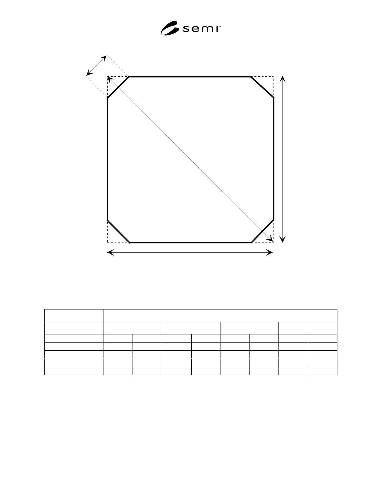
A
B
C
D
Figure 1
Rectangular Mainly Square Photovoltaic Solar Cell Silicon Wafer Dimensions
Table 2 Rectangular Mainly Square Photovoltaic Solar Cell Silicon Wafer Dimensions (letters as in Figure 1)
Nominal Size (mm) Dimensions (mm)
ABCD
Max. Min. Max. Min. Max. Min. Max. Min.
100 101 99 101 99 142.8 140.0 2.0 0.5
125 126 124 126 124 187.2 175.4 2.0 0.5
150 151 149 151 149 213.5 210.7 2.0 0.5
200 201 199 201 199 284.3 281.4 2.0 0.5
SEMI M6-1000 © SEMI 1981, 20007
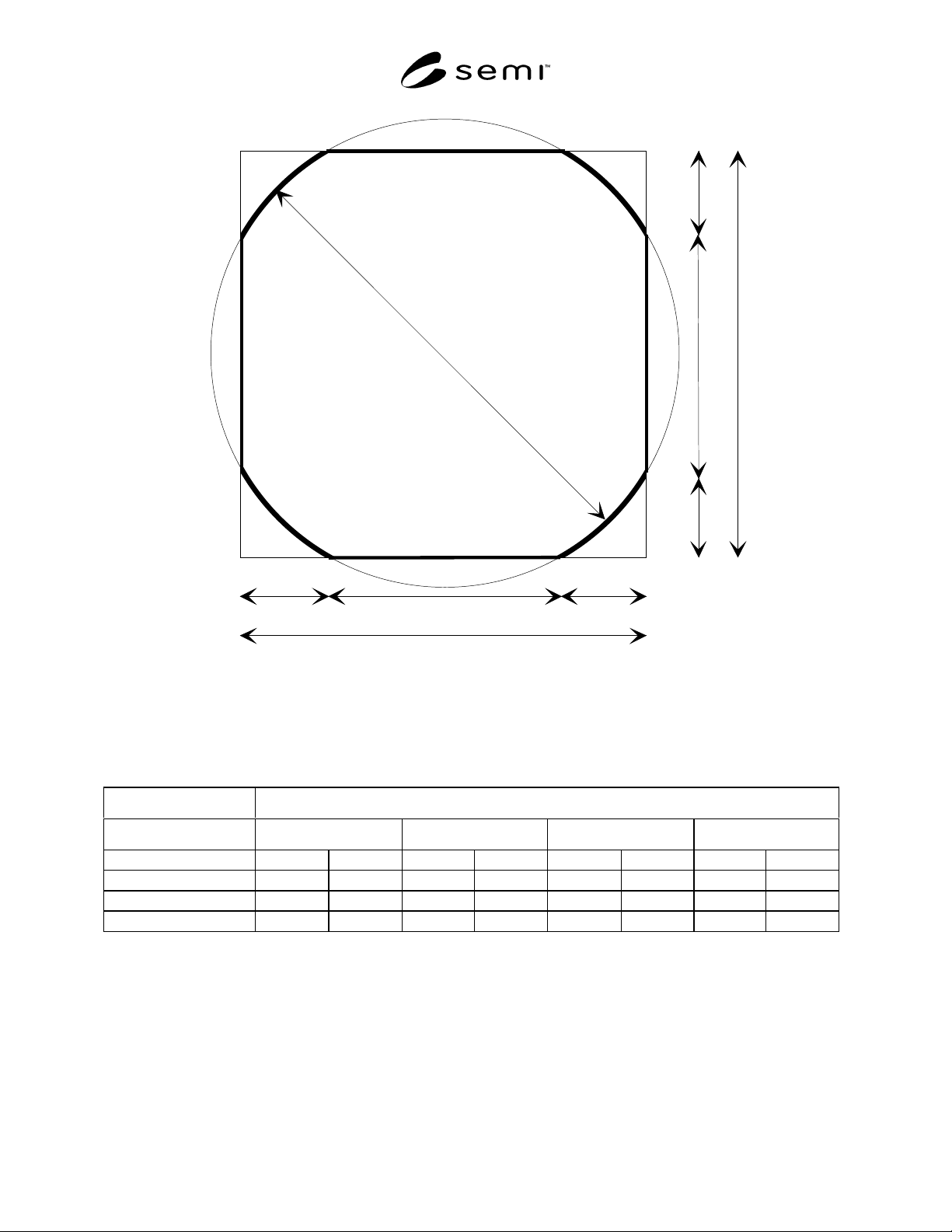
A
A
B
C
CDD
D
D
Figure 2
Pseudo-Square Monocrystalline Photovoltaic Solar Cell Silicon Wafer Dimensions
Table 3 Pseudo-Square Monocrystalline Photovoltaic Solar Cell Silicon Wafer Dimensions (letters as in
Figure 2)
Nominal size (mm) Dimensions (mm)
ABCD
Min. Max. Min. Max. Min. Max. Min. Max.
100 99 101 124 126 71.9 77.9 10.6 14.6
125 124 126 149 151 79.5 86.2 23.2 28.9
150 149 151 174 176 86.4 93.7 27.6 32.3

SEMI M6-1000 © SEMI 1981, 2000 8
APPENDIX 1
NOTE: The material in this appendix is an official part of SEMI M6 and was approved by full letter ballot procedures on July 28,
2000 by the European Regional Standards Committee.
A1-1 Crystal Orientation of Monocrystalline silicon
wafers
A1-1.1 A typical crystal orientation fo r monocrystal-
line silicon wafers is <100>.in the plane of the wafer.
A1-2 Wafer resistivity
A1-2.1 Typical wafer resistivity is between 0.5 Ω-cm
and 2 Ω-cm.
A1-3 Oxygen and Carbon Contents
A1-3.1 Typical values.
A-1.3.1.1 Interstitial oxygen < l × 10
l8
at /cm
3
for CZ
material and less than 8 × 10
17
at/cm
3
for multicrystal-
line wafers.
A-1.3.1.2 Substitutional carbon < 5 × 10
l7
at/cm
3
for
CZ and 1 × 10
l8
at/cm
3
for multicrystalline material.
A1-4 Lifetime and Minority Carrier Diffusion Length
A1-4.1 Typical minority carrier lifetim e values for
wafers used in the solar cell manufacturing process lie
in a range between 1 µs and 20 µs.
NOTICE: SEMI makes no warranties or
representations as to the suitability of the guidelines set
forth herein for any particular application. The
determination of the suitability of these guidelines is
solely the responsibility of the user. Users are cautioned
to refer to manufacturer’s instructions, product labels,
product data sheets, and other relevant literature
respecting any materials mentioned herein. These
guidelines are subject to change without notice.
The user’s attention is called to the possibility that
compliance with this standard may require use of
copyrighted material or of an invention covered by
patent rights. By publication of this standard, SEMI
takes no position respecting the validity of any patent
rights or copyrights asserted in connection with any
item mentioned in this standard. Users of this standard
are expressly advised that determination of any such
patent rights or copyrights, and the risk of infringement
of such rights, are entirely their own responsibility.
Copyright by SEMI® (Semiconductor Equipment and Materials
International), 3081 Zanker Road, San Jose, CA 95134. Reproduction o
f
the contents in whole or in part is forbidden without express written
consent of SEMI.