semi合集-English.pdf - 第5014页
SEMI M17-0704 © SEMI 1990, 2004 5 NOTICE: SEMI makes no warranties or representations as to the suitability o f the standards set forth herein for any particular application. The determination of the suitability of the s…
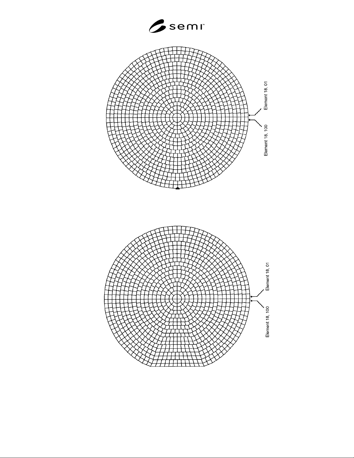
SEMI M17-0704 © SEMI 1990, 2004 4
Figure 1
Grid Layout for Wafers Without a Primary Flat
Figure 2
Grid Layout for Wafers With a Primary Flat

SEMI M17-0704 © SEMI 1990, 2004 5
NOTICE: SEMI makes no warranties or
representations as to the suitability of the standards set
forth herein for any particular application. The
determination of the suitability of the standard is solely
the responsibility of the user. Users are cautioned to
refer to manufacturer’s instructions, product labels,
product data sheets, and other relevant literature
respecting any materials mentioned herein. These
standards are subject to change without notice.
The user’s attention is called to the possibility that
compliance with this standard may require use of
copyrighted material or of an invention covered by
patent rights. By publication of this standard, SEMI
takes no position respecting the validity of any patent
rights or copyrights asserted in connection with any
item mentioned in this standard. Users of this standard
are expressly advised that determination of any such
patent rights or copyrights, and the risk of infringement
of such rights, are entirely their own responsibility.
Copyright by SEMI® (Semiconductor Equipment and Materials
International), 3081 Zanker Road, San Jose, CA 95134. Reproduction o
f
the contents in whole or in part is forbidden without express written
consent of SEMI.

SEMI M18-0704 © SEMI 1990, 2004 1
SEMI M18-0704
FORMAT FOR SILICON WAFER SPECIFICATION FORM FOR ORDER
ENTRY
This format was technically approved by the Global Silicon Wafer Committee and is the direct responsibility
of the Japanese Silicon Wafer Committee. Current edition approved by the Japanese Regional Standards
Committee on April 30, 2004. Initially available at www.semi.org June 2004; to be published July 2004.
Originally published in 1990; last published March 2004.
1 Purpose
1.1 This format provides a standard form for specifying
several classifications of silicon wafers, as follows:
1.1.1 Polished Silicon Wafers.
1.1.2 Epitaxial Silicon Wafers.
1.1.3 Epitaxial Silicon Wafers with Buried Layer.
1.1.4 Annealed Silicon Wafer.
1.1.5 SOI Wafers for CMOS Applications.
1.2 This format also lists the Electronic Data
Interchange (EDI) codes used in SEMI T6 to identify
the type of data being reported in the EDI message.
2 Scope
2.1 The form is designed to be used in conjunction
with other SEMI specifications where details of the
dimensional, physical, electrical, and chemical
properties are defined or specified. However, the form
includes many items that are not currently included in
the SEMI specifications. Also, many items are not now
commonly specified, but may find increased
importance in the future. The intention is to provide for
flexibility and expansion of the technology.
2.2 This format provides for specifying and ordering
silicon wafers with varying levels of complexity. The
minimum level of completeness is shown in each case,
with additional options included to allow for
customization of the wafer to the specific processing
requirements of the user. If a particular item is not of
interest, no entry is required. The only required entries
are those marked as such for the purpose of minimal
specification (diameter, orientation, dopant, resistivity,
etc.).
2.3 Values for many items are listed either in the
polished silicon wafer standards in SEMI M1 or in the
defect limits tables in SEMI M1, SEMI M2, or SEMI
M11. If these standard specifications are sufficient for
defining the wafers, only a single entry is required in
each section of the form.
2.4 This format also lists the codes required by SEMI
T6 to identify the parameter being reported in the EDI
message. Where necessary, secondary characteristics
or identifier codes are listed within a generalized
characteristic.
2.5 For referee purposes, U.S. Customary units shall be
used for wafers of 2- and 3-inch diameters, and SI
(System International, commonly called metric) units
for 100 mm and larger diameter wafers.
NOTICE: This standard does not purport to address
safety issues, if any, associated with its use. It is the
responsibility of the users of this standard to establish
appropriate safety and health practices and determine
the applicability of regulatory or other limitations prior
to use.
3 Referenced Standards
3.1 SEMI Standards
SEMI M1 — Specifications for Polished
Monocrystalline Silicon Wafers
SEMI M2 — Specifications for Silicon Epitaxial
Wafers for Discrete Device Applications
SEMI M11 — Specifications for Silicon Epitaxial
Wafers for Integrated Circuit (IC) Applications
SEMI M12 — Specification for Serial Alphanumeric
Marking of the Front Surface of Wafers
SEMI M13 — Specifications for Alphanumeric
Marking of Silicon Wafers
SEMI M20 — Specification for Establishing a Wafer
Coordinate System
SEMI M33 — Test Method for the Determination of
Residual Surface Contamination on Silicon Wafers by
Means of Total Reflection X-Ray Fluorescence
Spectroscopy (TXRF)
SEMI M35 — Guide for Developing Specifications for
Silicon Wafer Surface Features Detected by Automated
Inspection
SEMI M47 — Specification for Silicon-on-insulator
(SOI) Wafers for CMOS LSI Applications
SEMI MF26 — Standard Test Methods for
Determining the Orientation of a Semiconductive
Single Crystal