semi合集-English.pdf - 第7336页
SEMI MF1389-0704 © 2004 4 Boron Features, cm − 1 Phosphorus Features, cm − 1 B TO (b 2 ) = 8777.5 P TO (b 2 ′ ) = 8790.4 B B TO (b 3 ) = 8763.2 P TO (b 1 ) = 8778.0 C B TO (b 4 ) = 8752.1 P TO (b 3 ′ ) = 8771.3 B B TO (b…
SEMI MF1389-0704 © 2004 3
4.2 ASTM Standard
D 5127 — Guide for Ultra Pure Water Used in the
Electronics and Semiconductor Industry
7
NOTICE: Unless otherwise indicated, all documents
cited shall be the latest published versions.
5 Terminology
5.1 Definitions
5.1.1 defect luminescence lines — those features arising
from defect structures in the silicon.
5.1.2 electron hole droplet (EHD) — the condensed
phase (liquid) of the excitonic gas generated by
photoexcitation.
5.1.2.1 Discussion — The exciton population is
dependent upon excitation intensity and can be raised to
the point where the exciton density is sufficient to allow
condensation of the exciton gas into a liquid like
exciton state.
8
The existence of EHD luminescence can
be an indirect measurement of excitation power density
on the sample.
5.1.2.2 EHD onset occurs at the point in the sample
excitation intensity curve where the electron-hole-
droplet begins to form.
9
The EHD luminescence
includes a very broad feature underlying the TO region
impurity lines which, with increasing excitation
intensity, both intensifies and shifts to lower energies
relative to the other silicon luminescence features.
5.1.3 excitons — the electron-hole pairs that give rise to
the luminescence of interest upon recombination at
either a free lattice site (free exciton) or an impurity
atom site (bound exciton).
5.1.4 extrinsic line (X
TO
(BE) or X
NP
(BE)) — the
luminescence that arises from an exciton captured by an
impurity site in the crystal lattice (a bound exciton).
5.1.4.1 Discussion — Its energy is lower than the
intrinsic emission by an amount related to the exciton
binding energy of the impurity at 4.2 K. “X” is the
impurity element symbol and “BE” indicates bound
exciton luminescence line. Extrinsic luminescence also
includes features attributed to bound multi-exciton
complexes (b
1
, b
2
, or b
3
would indicate the first, second
and third bound multi-exciton complex lines,
respectively). In donor luminescence, these complexes
7 Annual Book of ASTM Standards, Vol 11.01, ASTM International,
100 Barr Harbor Drive, West Conshohocken, PA 19428. Telephone:
610-832-9500, Fax: 610-832-9555, Website:
www.astm.org.
8 Nakashima, H., and Shiraki, Y., “Role of Shallow Impurities and
Lattice Defects in Nucleation of Electron-Hole Droplets in Si,” Solid
State Comm. 40, 195–197 (1981).
9 Hammond, R. B., and Silver, R. N., “Onsets of the Electron-Hole
Droplet Luminescence in Si,” Phys. Rev. Lett. 42(8), 523–526 (1979).
give rise to two series of lines in the TO region, called
the alpha and beta series. The weaker beta series
features are denoted by an apostrophe after the line
notation (that is, P
TO
(b′
1
)). See Table 1 and Table 2 for
line locations.
5.1.5 intrinsic line (I
TO
(FE)) — the luminescence that
arises from the silicon itself, with no impurity species
affecting the exciton recombination.
10,11
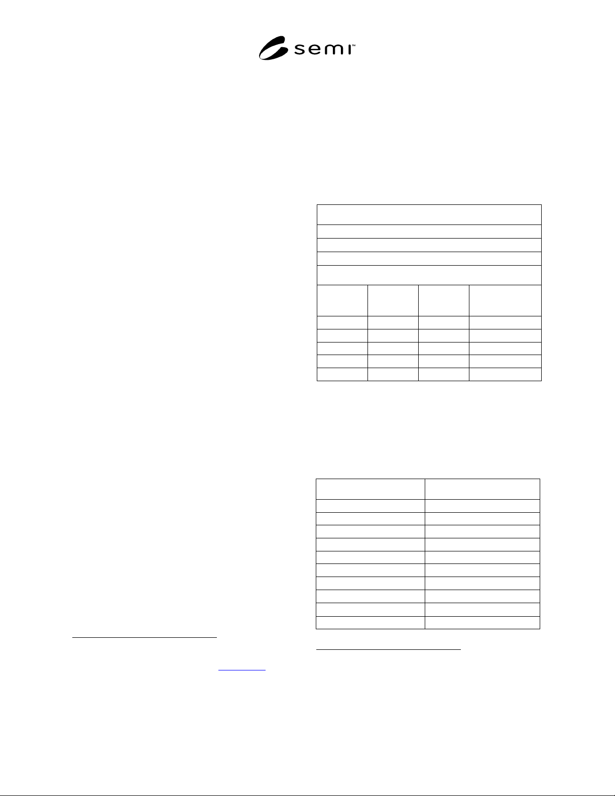
Table 1 Photoluminescence Line Locations
(Vacuum Wavenumbers)
Silicon Free Exciton (FE) Lines:
I
TO
(FE) at 8848 cm
−1
I
LO
(FE) at 8860 cm
−1
I
TA
(FE) at 9166 cm
−1
Major Shallow Impurity Bound Exciton (BE) Lines:
Element
TO region,
cm
−
1
NP region,
cm
−
1
NP/TO region BE
line intensity ratio
A
Boron 8812.6 9281.3 0.017
(Antimony) (8810.5) (9280.0) (0.010)
Phosphorus 8806.8 9275.4 1.4
Aluminum 8803.4 9271.8 0.7
Arsenic 8801.0 9269.4 2.0
NOTE 1: To convert vacuum wavenumbers to air wavenumbers:
air wavenumber = 1.00030025 × vacuum wavenumber
NOTE 2: To convert wavenumbers to electronvolts:
eV = 1.23985 × 10
−4
× wavenumber
A
Instrument resolution = 0.5 cm
−1
, sample = FZ silicon.
Table 2 Photoluminescence Line Locations
(Vacuum Wavenumbers) Detailed Listing for Boron
and Phosphorus
Boron Features, cm
−
1
Phosphorus Features, cm
−
1
B
NP
(BE) = 9281.3 P
NP
(BE) = 9275.4
B
NP
(b
1
) = 9263.6 P
NP
(b
1
) = 9246.4
B
NP
(b
2
) = 9245.9 P
NP
(b
2
) = 9223.9
P
NP
(b
3
) = 9208.4
P
NP
(b
4
) = 9197.8
B
TA
(BE) = 9130.1 P
TA
(BE) = 9124.4
B
TA
(b
1
) = 9112.4 P
NP
(BE-2e) = 8992.8
A
B
TA
(b
2
) = 9095.2
B
TO
(BE)= 8812.6
P
TO
(b
1
′) = 8812.7
B
B
TO
(b
1
) = 8795.0 P
TO
(BE) = 8806.8
C
10 Tajima, M., “Determination of Boron and Phosphorus Concen-
tration in Silicon by Photoluminescence Analysis,” Appl. Phys. Lett.
32(11), 719 (1978).
11 Tajima, M., “Quantitative Impurity Analysis in Si by the Photo-
luminescence Technique,” edited by J. Nishizawa, Japan Annual
Reviews in Electronics, Computers, and Telecommunications—
Semiconductor Technology (OHM—North Holland, 1982).

SEMI MF1389-0704 © 2004 4
Boron Features, cm
−
1
Phosphorus Features, cm
−
1
B
TO
(b
2
) = 8777.5
P
TO
(b
2
′) = 8790.4
B
B
TO
(b
3
) = 8763.2 P
TO
(b
1
) = 8778.0
C
B
TO
(b
4
) = 8752.1
P
TO
(b
3
′) = 8771.3
B
B
TO
(b
5
)= 8742.6 P
TO
(b
2
) = 8756.0
C
P
TO
(b
4
′) = 8756.2
B
P
TO
(b
5
′) = 8745.4
B
P
TO
(b
3
) = 8740.2
C
A
The two-electron transition is represented by 2e (see Ref (3)).
B
Beta series transition.
C
Alpha series transition.
5.1.5.1 Discussion — “I” indicates intrinsic silicon
emission, “TO” indicates the transverse optical phonon
associated with the transition, and “FE” refers to the
free exciton recombination responsible for the emission
(see Table 1 for line locations).
5.1.6 phonon — a quantum of lattice vibrational
energy, as a photon is a quantum of electromagnetic
energy.
5.1.6.1 Discussion — The recombination of excitons in
silicon requires a momentum conserving mechanism
owing to the indirect band gap of the crystal. Phonons
provide such a mechanism. The principal phonon types
of interest in silicon luminescence are the transverse
acoustic (TA), transverse optical (TO), and longitudinal
optical (LO) phonons. These test methods address the
use of features associated with the TO phonon as well
as those not including phonon emission in their
momentum-conserving processes. These latter features
are designated “NP” or no-phonon features.
6 Summary of Test Method
6.1 A sample of monocrystalline silicon is cooled to 4.2
K and photoexcited with greater-than-bandgap energy
light at one of two intensities listed, depending upon the
type of instrument used. The resulting luminescence is
collected and recorded. Spectral features corresponding
to intrinsic silicon and extrinsic impurity emissions are
measured and related to calibration curves to yield
dopant density.
7 Apparatus
7.1 Cryostat — To maintain sample temperature at 4.2
K. Either open-cycle liquid helium immersion or
exchange gas cryostats, or closed-cycle refrigeration
systems may be used. The bath immersion type
cryostat is recommended for higher confidence in the
temperature stability of the sample. In both the
exchange gas and closed-cycle systems, careful
attention must be paid to thermal sinking and accurate
sample temperature measurement (see Section 3.3).
7.2 Sample Holder — Which does not cause excessive
strain on the ample through spring forces or other
means, so as to avoid line splitting associated with
crystal stresses.
7.3 Laser Excitation Source — Capable of generating
electron hole pairs in the silicon crystal. An argon-ion
laser operated at 514.5 nm is used. To obtain accurate
measurements, laser light intensity must be controllable
and stable.
7.4 Infrared Spectrophotometer — Equipped with a
detector and optics suitable for use between 8750 and
9300 cm
−1
, and capable of at least 0.5 cm
−1
resolution at
9300 cm
−1
.
8 Reagents
8.1 Purity of Water — Reference to water shall be
understood to mean Type E-1 or better water as
described in ASTM Guide D 5127.
8.2 Nitric Acid (HNO
3
), 65%, in accordance with Grade
2 of SEMI C35.
8.3 Hydrofluoric Acid (HF), 48%, in accordance with
Grade 2 of SEMI C28.
8.4 Hydrogen Peroxide (H
2
O
2
), 30%, in accordance
with Grade 2 of SEMI C30.
8.5 Acid Cleaning Mixture, (1:1:1:25) HNO
3
:HF:H
2
O
2
:
H
2
O.
8.6 Hazards — Chemicals used in this procedure are
potentially harmful and must be handled with the
utmost care at all times.
9 Sample Preparation
9.1 Perform either the procedure in Section 9.1.1 or the
procedure in Section 9.1.2 to remove all work damage
and surface contamination on all samples except as-
received chemical-mechanically polished wafers, which
do not need further preparation.
9.1.1 Etch sample using a suitable etchant (for example,
the acid cleaning mixture of Section 8.5 or CP-5
hydrofluoric-nitric-acetic acid etchant).
9.1.2 Polish the surface of the sample with a suitable
chemical-mechanical polishing compound.
9.2 Luminescence efficiency has been observed to
decrease after etching, thus introduction of the sample
into the cryostat within a few hours of etching is
recommended. Chemical-mechanically polished
samples appear to be more stable.
2
SEMI MF1389-0704 © 2004 5
10 Instrument Calibration
10.1 Measurement of silicon standards need only be
performed once unless instrument characteristics have
drifted or hardware changes have been made. The
regular use of secondary standard samples, herein
referred to as audit samples, provides a mechanism for
instrument calibration verification and generates long-
term instrument performance statistics. At least four
standard samples should be used for each impurity
calibration curve adjustment.
10.1.1 Obtain samples with known impurity densities
and collect luminescence spectra at the appropriate
excitation intensity listed in Section 11.1 using both
standard and high resolution as listed in Section 11.2.2.
10.1.2 Find the peak intensities as described in Section
12 and find the ratios of appropriate spectral lines as
described in Section 13.1.
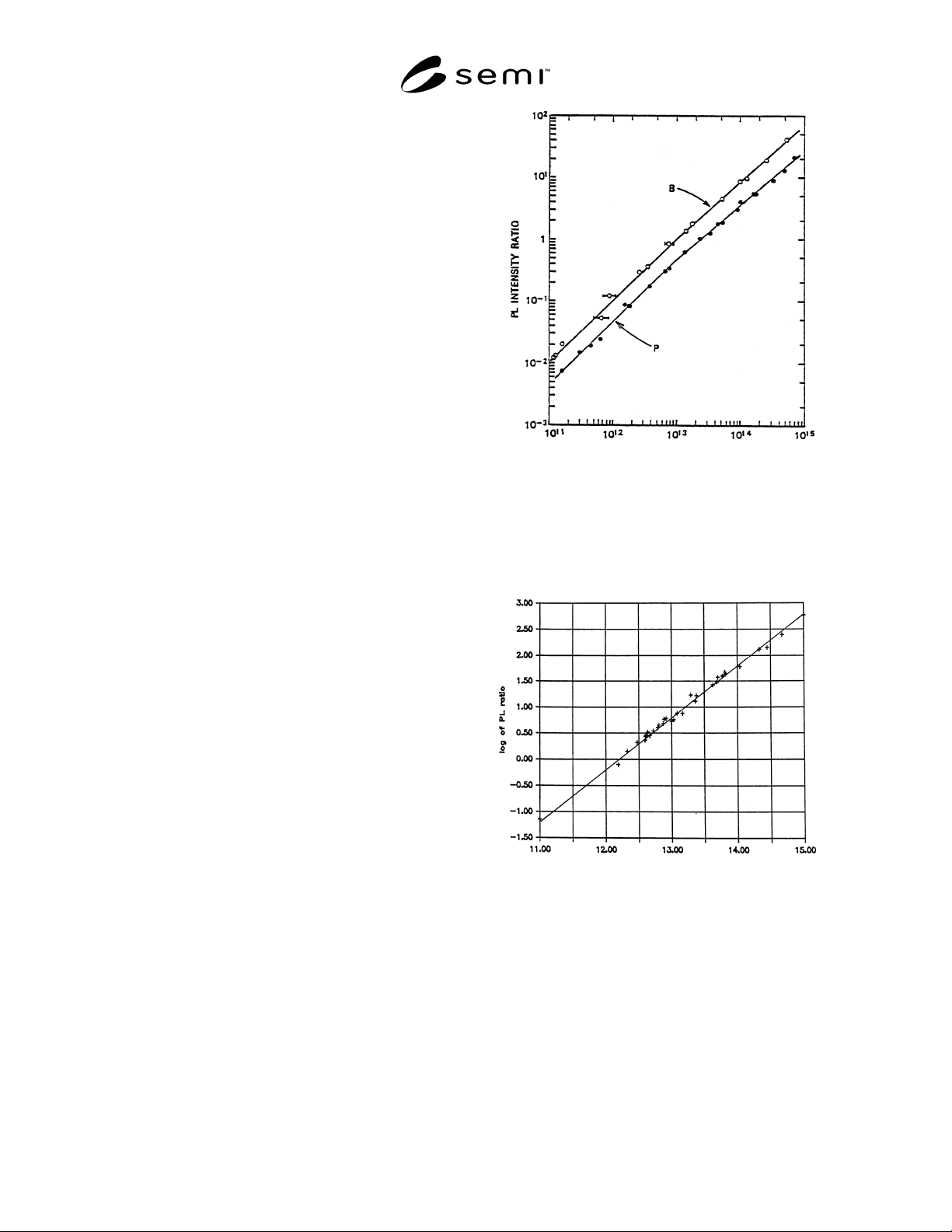
10.1.3 Adjust calibration data of Figure 1 or Figure 2,
corresponding to Test Method A or Test Method B,
respectively, by translating the curves such that they
intersect points corresponding to PL data of the known
samples. Make no change to the slope of the curves
because the slopes are a function of the exciton
recombination dynamics only and are independent of a
given instrument’s optical response.
10.1.4 These curves become the given instrument’s
calibration curves for the analysis conditions used.
10.2 Determine the short-term one-sigma precision of
the instrument.
NOTE 3: This procedure needs to be performed only
occasionally unless instrument characteristics have drifted or
hardware changes have been made.
10.2.1 Analyze a sample with impurity concentrations
similar to typical samples analyzed by the instrument in
normal operation nine times.
10.2.2 Find the peak intensity as described in Section
12 to obtain dopant densities.
10.2.3 Calculate the open-sigma standard deviation for
all impurities present.
11 Procedure
11.1 Excitation Conditions
11.1.1 Test Method A—High Excitation Intensity
Conditions — Set the output of the argon ion laser to
300 mW of 514.5 nm light. Pass the beam through an
infrared cutoff filter and a chopper with a 50% duty
cycle. Beam can be reflected with 2 to 3 mirrors with a
nominal 1-m distance between sample and laser. Pass
the unfocused beam through the cryostat windows. Set
the beam diameter to 2.5 mm.
DOPAN T DEN SI TY (c m
−
3
)
NOTE: The PL intensity ratio of P
TO
(BE)/I
TO
(FE) and
B
TO
(BE)/I
TO
(FE) are plotted against the P and B dopant
densities, respectively.
11
Figure 1
High Excitation Condition Impurity Calibration
Curves for Boron and Phosphorus (Test Method A)
log of dopa nt de nsit y (c m
−
3
)
NOTE: Slope = 1.0.
Figure 2
Low Excitation Condition Generic Impurity
Calibration Curve (Test Method B)
11.1.2 Test Method B—Low Excitation Intensity
Conditions — Set laser intensity such that the
luminescence is as close to the EHD onset point as
practical from signal-to-noise considerations. Collect
luminescence spectra of the sample used in Section
10.2 at several different laser beam intensities,
extending from well above to as far below the EHD