semi合集-English.pdf - 第6443页
SEMI G75.13-06 98 © SEMI 1998 3 5 Procedure 5.1 Setu p the test circuit as sho wn i n Figure 2. Figure 2 Test Circuit for Measurement of Leakage Current 5.2 P lace the f irst m olded sample i n th e shielded box and atta…
SEMI G75.13-0698 © SEMI 1998 2
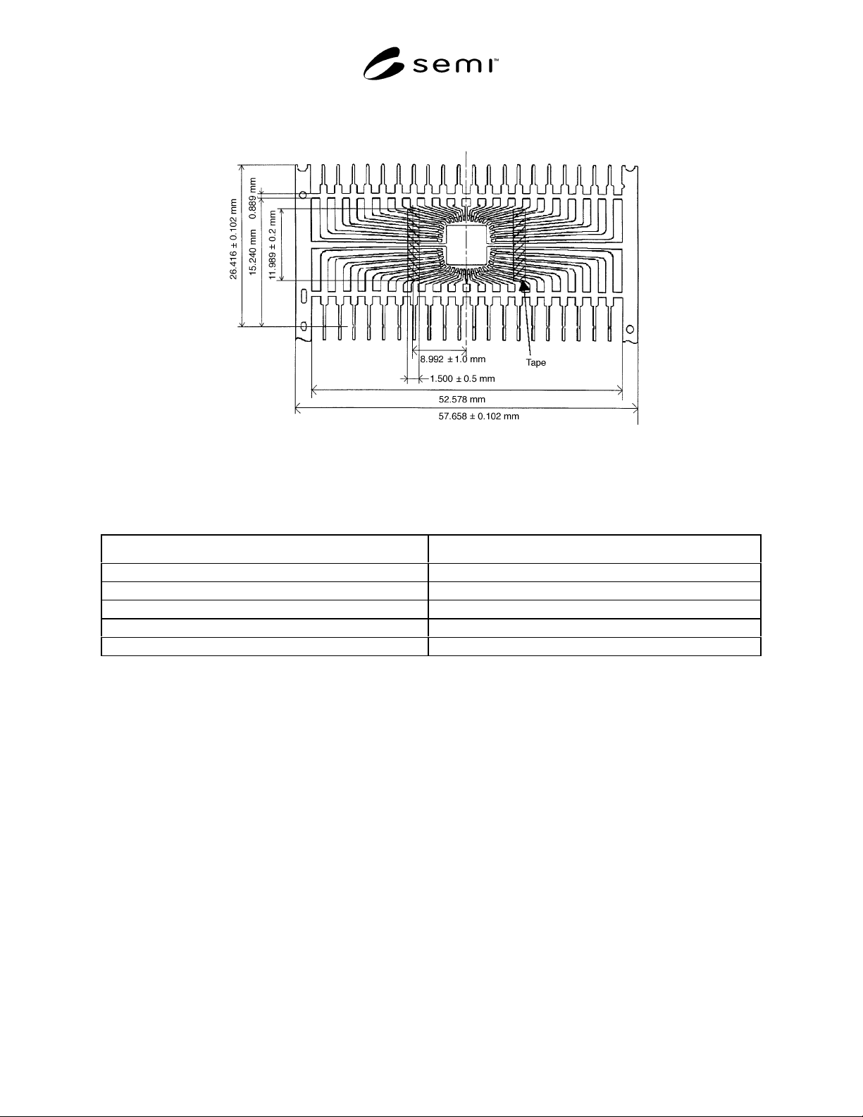
Figure 1
Typical Taped 40 Pin DIP Leadframe
Table 1 Relevant Information for 40 Pin DIP Leadframe
Leadframe Attribute Specification
Leadframe thickness 0.25 mm
Leadframe material Alloy 42
Leadframe manufacturing process Stamping
Plating None/Silver/Others
Surface treatment To be agreed between tape user and supplier.
NOTE 2: The surface state of Alloy 42 is stable compared with Cu alloy, which is oxidized easily.
4.3 The leadframes shall be molded using molding compounds and cured with post mold curing conditions agreed
on between vendor and customer. The untaped leadframe shall be prepared with the same procedure as a control.
4.4 Trim the leads according to a procedure agreed on between vendor and customer.
SEMI G75.13-0698 © SEMI 19983
5 Procedure
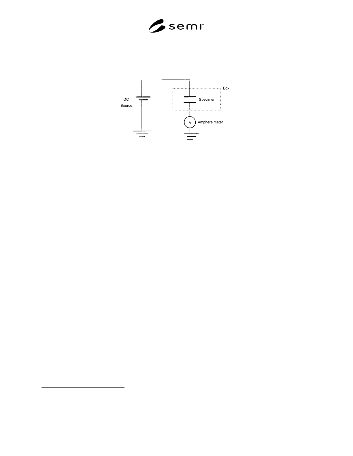
5.1 Setup the test circuit as shown in Figure 2.
Figure 2
Test Circuit for Measurement of Leakage Current
5.2 Place the first molded sample in the shielded box and attach clips to the leads A
1
and A
2
(see Figure 1).
Measure the initial leakage current at 500 volts maximum.
NOTE 3: The leakage current shall be measured after 5 minutes voltage application.
5.3 Repeat the measurement for all the lead pairs, A
2
with A
3
, B
1
with B
2
, and B
2
with B
3
.
5.4 Place the samples in the HAST chamber and run the test.
5.5 After the tester has been automatically cooled to room temperature, remove the samples.
5.6 Measure the leakage current between the same lead pairs mentioned in Sections 5.2 and 5.3.
5.7 Repeat the HAST exposure and measure the cur-rent leakage.
5.8 Calculation
5.8.1 Maximum and minimum leakage current shall represent the test results.
5.8.2 Calculate the average result for all of the test points at each test stage.
5.8.3 Obtained data should be converted to 100 volts basis or as agreed on between vendor and customer.
6 Related Documents
6.1 ASTM Specification
1
ASTM D 257 — Test Methods for D-C Resistance or Conductance of Insulating Materials
6.2 JIS Specification
2
JIS K 6911 — Testing Methods for Thermosetting Plastics
1 American Society of Testing and Materials, 100 Barr Harbor Drive, West Conshohoken, PA 19428-2959 (all cited standards may be found in
Volume 10.05 of the Annual Book of ASTM Standards)
2 Japanese Standards Association, 1-24, Akasaka 4 Chome, Minato-ku, Tokyo, Japan

SEMI G75.13-0698 © SEMI 1998 4
NOTICE: These standards do not purport to address
safety issues, if any, associated with their use. It is the
responsibility of the user of these standards to establish
appropriate safety and health practices and determine
the applicability of regulatory limitations prior to use.
SEMI makes no warranties or representations as to the
suitability of the standards set forth herein for any
particular application. The determination of the
suitability of the standard is solely the responsibility of
the user. Users are cautioned to refer to manufacturer’s
instructions, product labels, product data sheets, and
other relevant literature respecting any materials
mentioned herein. These standards are subject to
change without notice.
The user’s attention is called to the possibility that
compliance with this standard may require use of
copyrighted material or of an invention covered by
patent rights. By publication of this standard, SEMI
takes no position respecting the validity of any patent
rights or copyrights asserted in connection with any
item mentioned in this standard. Users of this standard
are expressly advised that determination of any such
patent rights or copyrights, and the risk of infringement
of such rights, are entirely their own responsibility.
Copyright by SEMI® (Semiconductor Equipment and Materials
International), 3081 Zanker Road, San Jose, CA 95134. Reproduction o
f
the contents in whole or in part is forbidden without express written
consent of SEMI.