semi合集-English.pdf - 第6458页
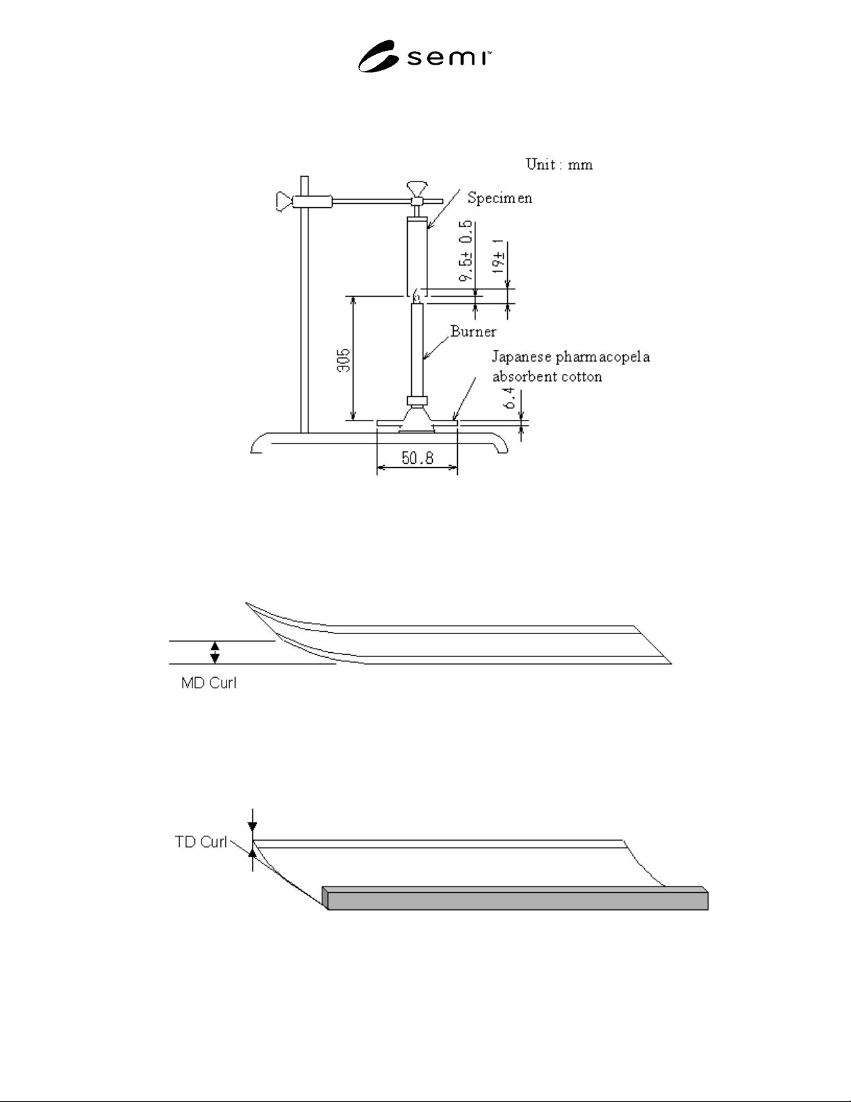
SEMI G76-0299 © SEMI 1999 14 Figure 6 Measurement of Flammability Figure 7 MD Curl Figure 8 TD Curl
SEMI G76-0299 © SEMI 1999 13
11.3 IEC Standards
3
249-1 Base Materials for Printed Circuits, Part 1: Test Methods
326-2 Printed Boards, Part 2: Test Methods
674-2 Specification for Plastic Films for Electrical Purposes, Part 2: Method of Test
11.4 UL Standard
4
94-1991 Standard for Flammability Tests of Plastic Materials for Parts in Devices and Appliances
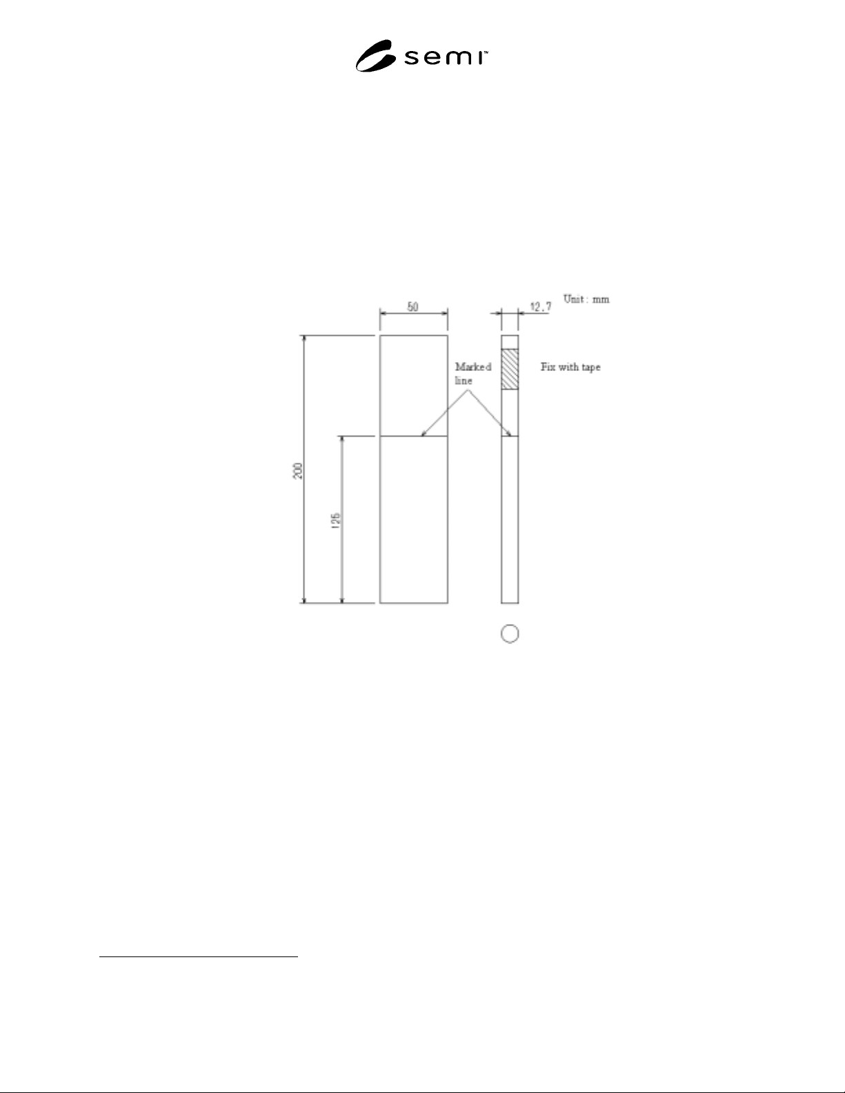
Figure 5
Test Specimen for Flammability
3 International Electrotechnical Commission, 3, rue de Varembé, P.O. Box 131, CH-1211 Geneva 20, Switzerland
4 Underwriters Laboratories, 333 Pfingsten Road, Northbrook, IL 60062-2096
SEMI G76-0299 © SEMI 1999 14
Figure 6
Measurement of Flammability
Figure 7
MD Curl
Figure 8
TD Curl
SEMI G76-0299 © SEMI 1999 15
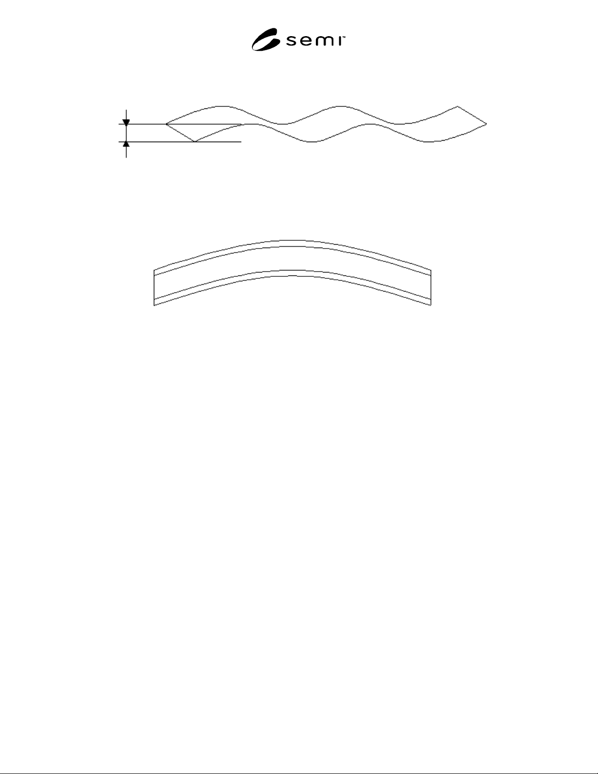
Figure 9
Wakame
Figure 10
Camber
NOTICE: These standards do not purport to address safety issues, if any, associated with their use. It is the
responsibility of the user of these standards to establish appropriate safety and health practices and determine the
applicability of regulatory limitations prior to use. SEMI makes no warranties or representations as to the suitability
of the standards set forth herein for any particular application. The determination of the suitability of the standard is
solely the responsibility of the user. Users are cautioned to refer to manufacturer' s instructions, product labels,
product data sheets, and other relevant literature respecting any materials mentioned herein. These standards are
subject to change without notice.
The user' s attention is called to the possibility that compliance with this standard may require use of copyrighted
material or of an invention covered by patent rights. By publication of this standard, SEMI takes no position
respecting the validity of any patent rights or copyrights asserted in connection with any item mentioned in this
standard. Users of this standard are expressly advised that determination of any such patent rights or copyrights, and
the risk of infringement of such rights, are entirely their own responsibility.
Copyright by SEMI® (Semiconductor Equipment and Materials
International), 3081 Zanker Road, San Jose, CA 95134. Reproduction o
f
the contents in whole or in part is forbidden without express written
consent of SEMI.