semi合集-English.pdf - 第6488页
SEMI G79-0200 © SE MI 2000 1 SEMI G79-0200 SPECIFICA TION FOR OVERALL DIGITA L TIMING ACCURAC Y This specifica tion w as technic ally approv ed by the G lobal A utomated T est Equipm ent Committe e and is the direct resp…
SEMI G78-0699 © SEMI 1999 20
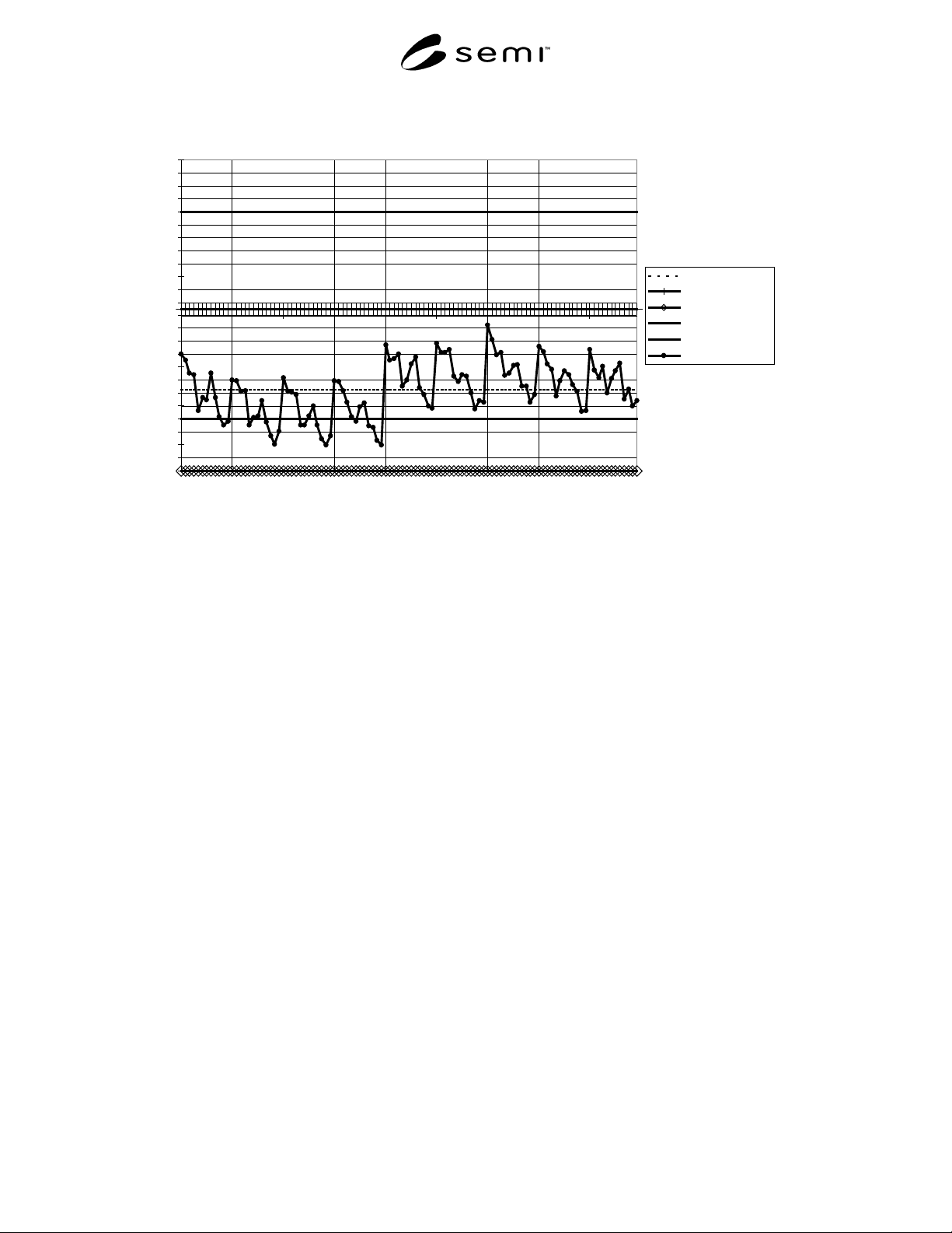
Avg Lot Y-Offset
Avg Lot Y-Offset +3s
Avg Lot Y-Offset -3s
Lower Spec Limit
Upper Spec Limit
Average Die Y-Offset
Figure 8
Y-Offset
NOTICE: These standards do not purport to address
safety issues, if any, associated with their use. It is the
responsibility of the user of these standards to establish
appropriate safety and health practices and determine
the applicability of regulatory limitations prior to use.
SEMI makes no warranties or representations as to the
suitability of the standards set forth herein for any
particular application. The determination of the
suitability of the standard is solely the responsibility of
the user. Users are cautioned to refer to manufacturer’s
instructions, product labels, product data sheets, and
other relevant literature respecting any materials
mentioned herein. These standards are subject to
change without notice.
The user’s attention is called to the possibility that
compliance with this standard may require use of
copyrighted material or of an invention covered by
patent rights. By publication of this standard, SEMI
takes no position respecting the validity of any patent
rights or copyrights asserted in connection with any
item mentioned in this standard. Users of this standard
are expressly advised that determination of any such
patent rights or copyrights, and the risk of infringement
of such rights, are entirely their own responsibility.
Copyright by SEMI® (Semiconductor Equipment and Materials
International), 3081 Zanker Road, San Jose, CA 95134. Reproduction o
f
the contents in whole or in part is forbidden without express written
consent of SEMI.

SEMI G79-0200 © SEMI 20001
SEMI G79-0200
SPECIFICATION FOR OVERALL DIGITAL TIMING ACCURACY
This specification was technically approved by the Global Automated Test Equipment Committee and is the
direct responsibility of the North American Automated Test Equipment Committee. Current edition approved
by the North American Regional Standards Committee on September 3, 1999. Initially available at
www.semi.org November 1999; to be published February 2000.
1 Purpose
1.1 This standard is intended to provide a minimum
common definition of timing accuracy specifications
for automatic semiconductor test equipment (ATE).
2 Scope
2.1 The scope of this standard includes all semicon-
ductor ATE capable of digital functional testing. This
standard does not include the following:
• test fixturing errors,
• device insertion errors, and
• ATE performance or capability beyond timing
accuracy.
2.2 This standard’s overall timing accuracy (OTA)
definition serves to simplify automatic test equipment
comparisons and reduce specification ambiguity.
2.3 This standard does not purport to address safety
issues, if any, associated with its use. It is the responsi-
bility of the users of this standard to establish appro-
priate safety and health practices and determine the
applicability of regulatory limitations prior to use.
3 Limitations
3.1 Parameters associated with the following items are
not covered by the Overall Digital Timing Accuracy
Specification:
• minimum driver pulse width,
• comparator bandwidth,
• I/O round trip delay,
• test fixturing errors,
• device insertion errors,
• time measurement unit accuracy, and
• ATE capability or performance beyond timing
accuracy.
4 Referenced Standards
None.
5 Terminology
5.1 Abbreviations and Acronyms
5.1.1 ATE — automatic test equipment
5.1.2 DUT — device under test
5.1.3 NR — Non-return signal format
5.1.4 RTx — return to zero, one or complement signal
format.
5.1.5 SBx — surround by zero, one or complement
signal format.
5.1.6 Z — driver off (high impedance)
5.2 Definitions
5.2.1 device insertion errors — error influenced by
device-input capacitance and/or terminations.
5.2.2 edge — time delay created by an ATE delay
generation resource.
5.2.3 performance board — printed circuit board used
to interface the tester channels to the device under test.
5.2.4 pin — tester channel
5.2.5 reference load A — 500 ohms in parallel with
2.5pf (± 0.5pf) to ground
5.2.6 reference load B — 50 ohms to ground
5.2.7 reference load C —
• 50 ohms to low (for driver z to high and high to z
transitions).
• 50 ohms to high (for driver z to low and low to z
transitions).
5.2.8 strobe compare — monitor DUT output at a
single time point.
5.2.9 test cycle — inverse of test pattern execution
frequency.
5.2.10 test fixturing errors — error influenced by
mismatched signal path lengths, impedance discontinu-
ities, lumped capacitance/inductance elements, and high
frequency loss due to skin effect or interconnects.
5.2.11 window compare — monitor DUT continuously
during a time interval.
SEMI G79-0200 © SEMI 2000 2
NOTE 1: The term “input” as it appears in this document
refers to the device under test.
6 Test Methods
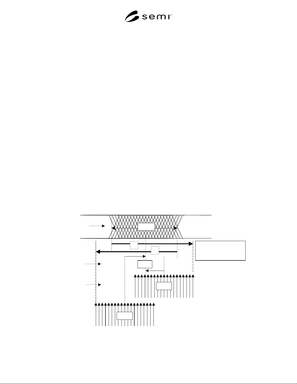
6.1 See Figure 1.
NOTE 2: A verification procedure to complement this Overall
Digital Timing Accuracy Specification is currently being
developed as a SEMI draft document.
6.2 Explanation of Figure 1 — This figure is meant to
graphically describe Overall Timing Accuracy and its
constituent components. Overall Timing Accuracy
(OTA) is made up of three components, and by
definition is the aggregate timing error comprised of
input edge placement accuracy (see Section 7.1.1),
output edge placement accuracy (see Section 7.1.2), and
input to output timing accuracy (see Section 7.1.3). It’s
important to note that the OTA specification and
associated graphical representation shown in Figure 1 is
meant to encompass timing delay errors across multiple
machines, as well as multiple calibrations for a single
machine over time.
6.2.1 Our experience in dealing with multiple-pin
automated test systems reveals that not all input drive
circuits can place a drive edge at exactly the same point
in time relative to a common reference. The same is
true for output compare circuits when placing compare
edges. Thus, these edges tend to have an (error)
distribution around some average value relative to their
intended placement. This is due in part to the inherent
anomalies associated with electronic circuits that make-
up these edge placement elements. The distribution of
edge error is graphically shown for input (see Section
7.1.1) and output edge (see Section 7.1.2) signals in
Figure 1.
6.2.2 Drive Input to Compare Output Timing
Accuracy (Section 7.1.3) can be described in different
ways. It is easy to think of this parameter, per the
definition given in this document, Section 7.1.3, as
simply the relative time difference (skew) between the
drive delay timing error distribution and the compare
delay timing error distribution for a particular machine.
But this parameter, once established for a machine, is
not necessarily constant. For example, this parameter
can change from one calibration of a machine at a
particular time, to something different, as a result of a
subsequent calibration of that same machine. As well,
this parameter can also be considered as a machine to
machine accuracy parameter, not necessarily having the
same value between any two machines of the same
kind.
6.2.3 Thus, on each machine and at different points in
time for the same machine the Drive Input to Compare
Output Timing skew can be uniquely different per
machine. That difference being influenced by the
various machine anomalies that contribute to machine
error including the not so perfect results of a periodic
edge calibration.
7.1.2
Input to Output Timing
Accuracy (7.1.3)
Output Edge Placement
Accuracy (7.1.2)
7.1.3
Input Edge Placement
Accuracy (7.1.1)
7.1.1
Output delay timing error- For another machine,
or a new spread for the same machine as a result
of a calibration.
7.1.2
Output timing delay
error.
A
B
Overall Timing Accuracy
(+A, -B)
Figure 1
Overall Timing Accuracy