semi合集-English.pdf - 第968页
SEMI E129-1103 © SEMI 2003 6 8 Safety Precautions 8.1 Personnel — Static charges can create safety hazards during som e semiconductor production processes. 8.1.1 ESA, ESD, and EMI events that result in the jamming or bre…
SEMI E129-1103 © SEMI 2003 5
E43. There are currently no industry standards for
determining the electric field sensitivity of reticles, but
test methods do exist.
6.3.4 Finally, there is increasing anecdotal evidence
that the presence of static charge on wafer surfaces is
becoming an ESD hazard as gate oxide thicknesses
become thinner. In the future, there may need to be
further limits on allowable static charge on wafer
surfaces to prevent ESD-related gate oxide damage
during front-end semiconductor manufacturing. Further
research is needed in this area.
6.4 Particle Attraction
6.4.1 Electrostatic attraction (ESA) of particles can
occur due to the electrostatic field created by the charge
on the surface of an object. Refer to SEMI E78 and
SEMI E43 for an analysis of this effect and its
measurement methods.
6.4.2 Particles may be attracted to charged facility
surfaces, or directly to charged products or reticles.
Subsequently, they may be dislodged from facility
surfaces and transfer to products or reticles. Once on
products or reticle surfaces they may cause either
random or repeating defects.
6.4.3 Electrostatic particle deposition velocity depends
only on electric field, particle size and particle charge.
However, the number of particles deposited on a
surface also depends on the particle concentration in the
area and the length of the exposure time during which
particle deposition occurs. SEMI E78 contains
information to relate allowable electric field to ambient
particle concentration and exposure time.
6.4.4 The measurement methods of SEMI E43 can be
used to establish that the electric field from any facility
surface meets the requirements of this document.
6.4.5 Charge is difficult to evaluate on large objects,
especially insulators. Electric field measurements on
these objects may be useful in estimating the risk that a
damaging direct ESD event might occur. However,
electric field measurements on insulators are highly
qualitative and only provide a figure of merit as to the
threat that these charges may represent to the ESD-
sensitive device.
6.5 Equipment ESD
6.5.1 Equipment ESD immunity has been established
at levels considerably higher than those that result in
damage to product and reticles. If facility static charge
limits shown in Table 1, of Section 12.5 are used to
protect product and reticles, they will provide sufficient
protection for the equipment.
6.5.2 Equipment ESD immunity is addressed, in
general, through a number of international standards
including SEMI E78, IEC 61000-4-2, and BS
EN50082-2 for European CE compliance.
Measurements are made using an ESD simulator, which
is described in these standards.
7 Apparatus
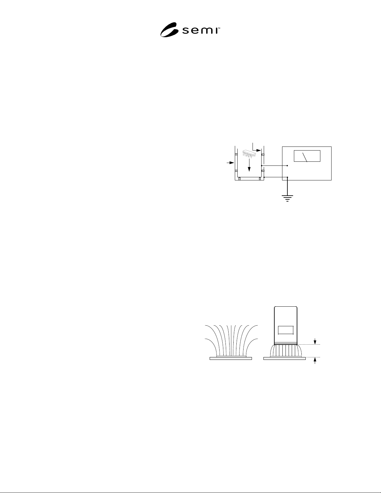
7.1 ESD Damage — For measuring the charge
generated on product, reticles, or carriers, the Faraday
Cup test method is shown in Figure 1. Additional
information on this test method is contained in SEMI
E43.
In
Ground
Electrometer
Faraday
Cup
Isolated
Inner Cup
Shielding
Outer Cup
Figure 1
Faraday Cup Charge Measurement
7.2 When the object whose charge is to be measured is
conductive, a nanocoulombmeter may be used.
Additional information on this test method is contained
in SEMI E43.
7.3 The instrument used for making electrostatic field
measurements on large objects or surfaces is known as
an electrostatic fieldmeter. Instructions concerning its
use should be obtained from the instrument
manufacturer and SEMI E43. The measurement
configuration is shown in Figure 2.
1
9
9
9
+ + + + + + + + + + + + + + + +
2.54 cm
(1 inch)
Electrostatic
Fieldmeter
(volts/cm)
+ + + + + + + + + + + + + + + +
Charged
Surface
Electric Field Lines
Charged
Surface
Figure 2
Electrostatic Field Measurement
7.4 For small objects or surface areas, an electrostatic
voltmeter is appropriate.

SEMI E129-1103 © SEMI 2003 6
8 Safety Precautions
8.1 Personnel — Static charges can create safety
hazards during some semiconductor production
processes.
8.1.1 ESA, ESD, and EMI events that result in the
jamming or breakage of product in high-speed
equipment may create a personnel hazard.
8.1.2 ESD events that produce sparks must be
prevented in areas that use flammable or explosive
chemicals or gases.
8.1.3 ESD events to personnel are usually not harmful,
but they may result in an unwanted reflex, or “startle”
reaction. This reflex may create a personnel hazard,
particularly in the vicinity of moving equipment or
where caustic chemicals are in use.
8.1.4 EMI resulting from ESD events may cause
unpredictable behavior of robotics or other moving
equipment that put personnel at risk.
8.1.5 It may be necessary to use additional static
charge control methods, beyond those used inside the
equipment, to minimize these personnel hazards.
8.2 Measurement Safety — Users should exercise
caution while making static charge measurements in the
vicinity of moving parts of production equipment, or in
areas where static potentials on ungrounded conductors
may exceed 30,000 V. Refer to SEMI E43 for
additional measurement safety considerations.
9 Test Specimen
9.1 The user, material supplier, facility
designer/builder, and equipment manufacturer should
agree upon and document:
• Type(s) of testing to be performed
• Location of the testing (e.g., in a test chamber or in
the actual use location)
• Who will do the testing
• Number and type of test samples
• Number of measurements
• Acceptable test results
9.2 The user, material supplier, facility
designer/builder, and equipment manufacturer should
agree upon and document all appropriate environmental
conditions (e.g., temperature, humidity, dew point,
airflow).
9.3 The user, material supplier, facility
designer/builder, and equipment manufacturer should
agree upon and document the operating history of
equipment prior to, or during testing (e.g., warm-up
time, type of carrier, number of products processed,
operating speed).
10 Preparation of Apparatus and Sample
10.1 Depending on the type of testing to be done,
consult the appropriate testing document for apparatus
and sample preparation. See Section 4.
11 Calibration and Standardization
11.1 Depending on the type of testing to be done,
consult the appropriate testing document for apparatus
calibration and verification. See Section 4.
12 Procedures
12.1 See Sections 6 and 7 and the appropriate test
methods of Section 4.
12.2 ESD Damage
12.2.1 Users should establish product damage
thresholds for their products. Measurement methods
for integrated circuits are described in SEMI E78
Related Information 1 and the documents contained in
Section 4. Appropriate measurement methods for ESD
damage to wafers, reticles, and other items may be
adapted from the instrumentation used in these test
methods.
12.2.2 In place of using the test methods referenced in
Section 12.2.1, users may decide to follow the
recommendations for acceptable electrostatic levels
contained in Section 12.5 Table 1, which are based on
product and reticle geometry. See Appendix 1 for more
information.
12.2.3 Measurements of ESD damage levels are made
in units of coulombs, or more conveniently in
nanocoulombs (nC = 10
-9
coulombs).
12.2.4 The Faraday Cup method is used to determine
the static charge levels on products, carriers and
equipment parts. See Section 7.1. Each item should be
transported to the Faraday Cup in a way that does not
alter its charge level. Consult the measurement
equipment manufacturer’s instructions for
recommendations on how to achieve this.
12.3 Electrostatic Field
12.3.1 Users should work with cleanroom designers,
material suppliers, equipment manufacturers and reticle
suppliers to determine ambient particle levels, product
exposure times during processing, and reticle damage
levels due to electric field.
12.3.2 Electrostatic field measurements should be
made at a minimum on all surfaces within the facility
SEMI E129-1103 © SEMI 2003 7
that will come within 30.5 cm (12 inches) of ESD-
sensitive items. Typical surfaces to measure would
include construction materials, furniture, personnel,
products, carriers, and equipment surfaces.
12.3.3 Measurements should be made in at least three
different locations on any item. Locations should be
separated by approximately three times the distance
between the measuring instrument and the measurement
location. For most electrostatic fieldmeters measuring
at 25.4 mm (1 inch), the measurement locations will be
76.2 mm (3 inches) apart. Refer to SEMI E43 for
additional measurement considerations.
12.3.4 Measurements of electrostatic field are
expressed in V/cm or V/inch. Typically, five
measurements should be sufficient to demonstrate
compliance with the selected electrostatic level.
12.4 All elements of the semiconductor factory,
including but not limited to construction materials,
furniture, equipment, personnel, product, reticles,
carriers, and transport and packaging materials, should
meet the following electrostatic levels shown in Section
12.5 Table 1 for protection from problems caused by
static charge.
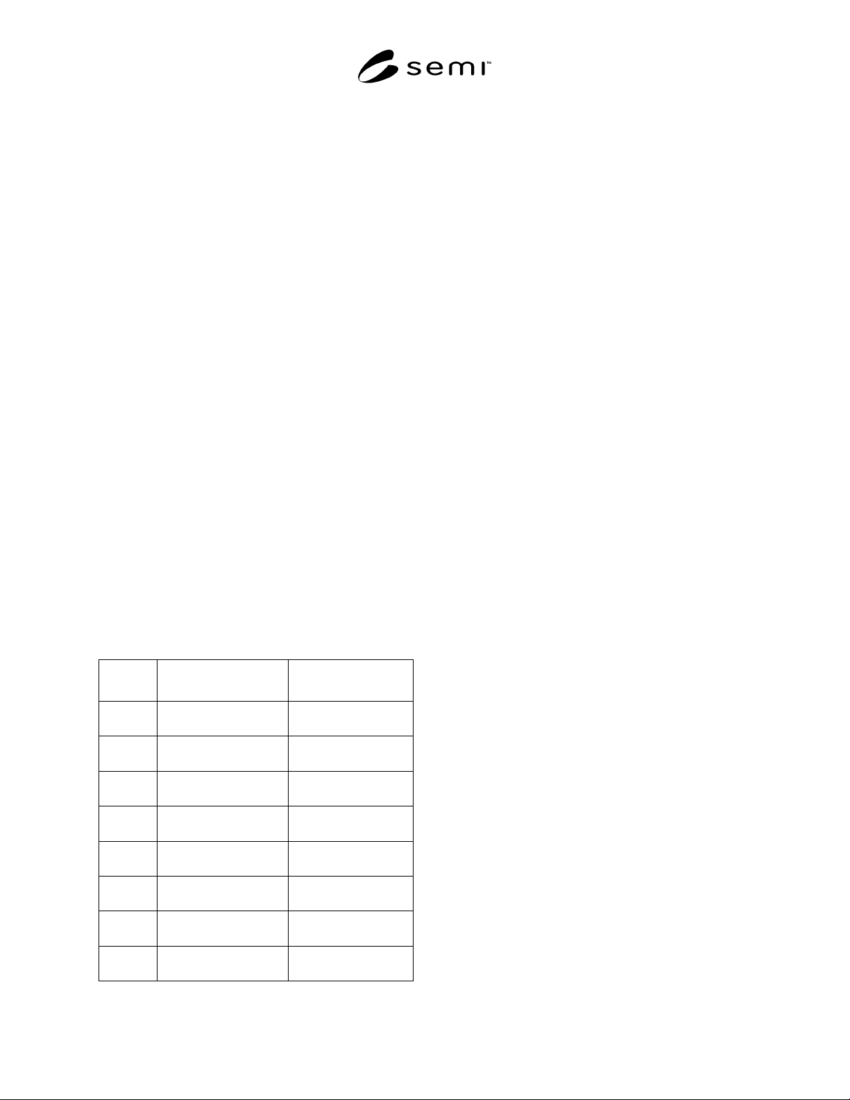
12.5 It is desirable in this document to avoid confusion
with SEMI E78 sensitivity levels, as well as to
synchronize with the major changes in technology
mapped in the International Technology Roadmap for
Semiconductors (ITRS). Recommendations for
acceptable static charge levels are listed in Table 1 and
given for the major technology nodes of the 2003 ITRS
that relate to the size of the features on the wafer.
Table 1 Recommended Facility Electrostatic Levels
Year
Node
Electrostatic Discharge,
nC
Electrostatic Field,
V/cm V/inch
2000
180 nm
2.5–10 200 500
2002
130 nm
2.0 150 375
2003
100 nm
1.5 125 300
2004
90 nm
1.0 100 250
2007
65 nm
0.5 70 175
2009
50 nm
0.25 50 125
2012
32 nm
0.125 35 88
2015
25 nm
0.1 25 63
12.5.1 Since many decisions to use static control
materials will result in the permanent installation of
these materials, users may want to consider the eventual
use of their semiconductor facility in selecting the
acceptable electrostatic level. For example, at startup
the facility may be processing at 180-nm geometry, but
in five years it is anticipated to be at 90 nm. The
facility may need to be designed for the limits
recommended for the 90-nm use.
12.5.2 The levels in Table 1 assume that the
manufacturing facility is processing silicon
semiconductors. Manufacturers of specialized
components may need to choose lower levels.
Examples are manufacturers of gallium arsenide
semiconductors or magneto-resistive (MR) disk drive
read heads, those experiencing significant losses due to
contamination, or those using specialized equipment.
12.6 The levels listed in Table 1 have been determined
as the result of an analysis of working conditions, or
experiments done in operating semiconductor facilities.
Justifications for these levels are found in Appendix 1.
The actual levels to be used for any production area
may be decided by agreement between the user and
designer/builder of the facility.
12.7 Other levels may be appropriate under specific
operating conditions and for specific devices.
13 Calculations
13.1 A series of five measurements should be made.
The average of the five measurements should not
exceed the recommended level. No measurement
should exceed two times the recommended level.
14 Reporting Results
14.1 Data records should contain the following
information:
• Description of the materials or equipment under
test including model and serial numbers,
• Description of the factory operating conditions and
environment,
• Measurement equipment and last calibration date,
• Description of objects measured and measurement
locations,
• Humidity, temperature, and dew point at
measurement location when measurements were
made,
• Results of measurements,
• Personnel making the measurements, and
• Any other relevant comments.