semi合集-English.pdf - 第6018页
SEMI G1-96 © SEMI 1 980, 199 6 11 A P PENDIX 1 CERAMIC CERDI P BA SE DIM ENSIONS A ND TOLER ANCE REQUIREM ENTS — STA ND ARD OUTLINES Table 2 Ceram ic Cerdip Base Dimen sions and Tolerance R equirements Lead Cou nt Min. L…

SEMI G1-96 © SEMI 1980, 1996 10
10.3.7.8 Condition A shall be performed to conditions
agreed upon between user and supplier.
11 Sampling
The sampling plan used at incoming inspection shall be
based on MIL-STD-105 and agreed upon between user
and supplier (see Figure 8).
12 Packaging, Marking, and Packing List
12.1 Packaging — The shipping containers and
materials shall be suitably designed to provide the
components or sub-assemblies with protection against
normal transportation damage risks which include
crushing, spillage, and exposure to moisture and other
corrosive gases.
The inner packaging materials must not cause
particulate contamination of the components or sub-
assemblies and shall be cleanroom compatible as
defined by the user. The components or sub-assemblies,
in packing trays, shall be vacuum-sealed in a bag with a
desiccant.
12.2 Marking
12.2.1 Internal Packages — Each internal package
shall be clearly marked with the following information,
as appropriate:
• User’s part number,
• User’s purchase order number,
• Drawing number (user’s and/or supplier’s, as
requested by user),
• Quantity, and
• Date of manufacture.
The package shall also contain any agreed upon
certification data.
12.2.2 External Packages — The packing list on the
outside of the external package shall contain the
following information:
• User’s part number,
• User’s purchase order number,
• Quantity,
• Shipping date, and
• Any specific instructions for receiving dock
personnel.
13 Certification
13.1 Upon request of the user in the contract or
purchase order, a supplier’s certification that the
product was manufactured and tested in accordance
with this specification, together with a report of the test
results, shall be furnished at the time of shipment.
However, if the user does perform inspection and test
on a certified shipment, and the product fails to meet
the requirements, the product shall be subject to
rejection.
13.2 If the user and supplier agree, the product may be
certified as capable of meeting this specification. In this
context, capable of meeting signifies that the supplier is
not required to perform all the inspections and tests.
However, if the user does perform inspection and test
on a certified shipment, and the product fails to meet
the requirements, the product shall be subject to
rejection.
SEMI G1-96 © SEMI 1980, 199611
APPENDIX 1
CERAMIC CERDIP BASE DIMENSIONS AND TOLERANCE
REQUIREMENTS — STANDARD OUTLINES
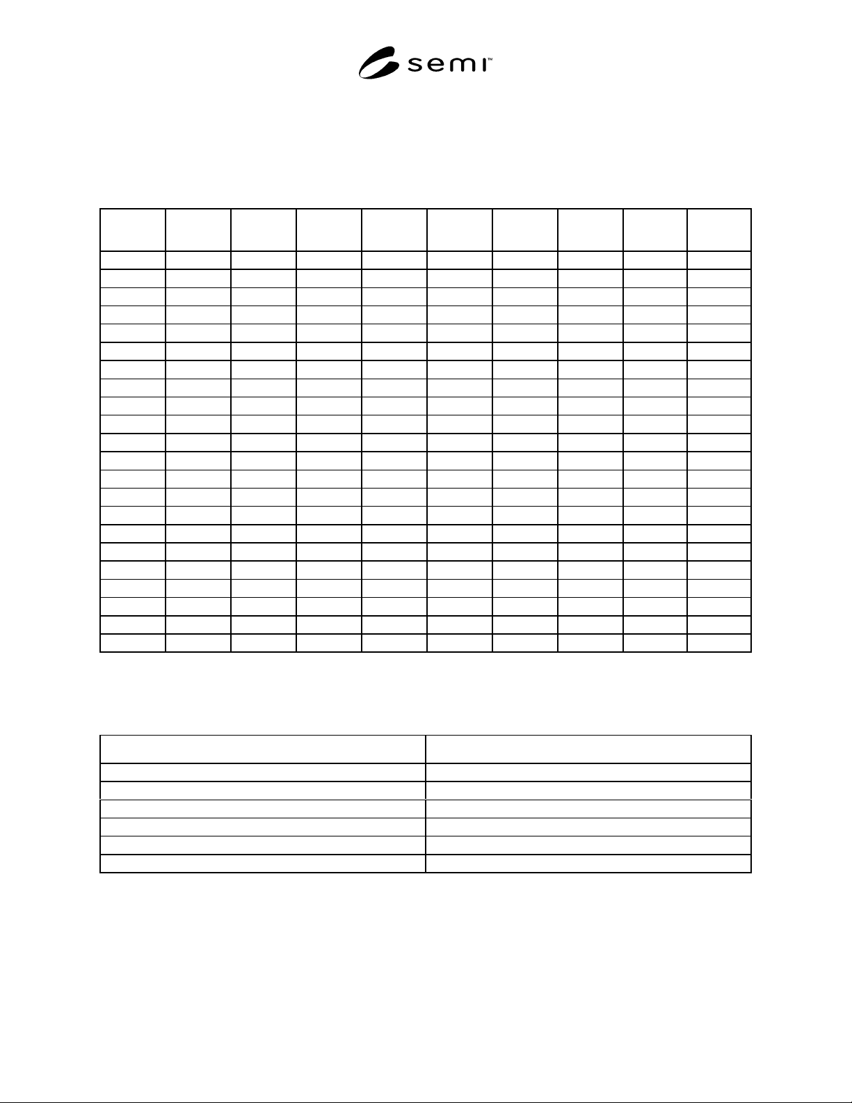
Table 2 Ceramic Cerdip Base Dimensions and Tolerance Requirements
Lead Count Min. Length Max. Length Min. Width Max. Width
Min. Cavity
Length
Max. Cavity
Length
Min. Cavity
Length
Max. Cavity
Length Units
8 0.380 0.400 0.248 0.288 0.140 0.220 0.120 0.380 in
9.65 10.16 6.29 7.31 3.55 5.58 3.04 9.65 mm
14 0.760 0.750 0.248 0.288 0.140 0.250 0.110 0.150 in
19.30 19.30 6.29 7.31 3.55 6.35 2.79 3.81 mm
16 0.760 0.760 0.248 0.288 0.140 0.400 0.110 0.193 in
19.30 19.30 6.28 7.31 3.55 10.16 2.79 4.90 mm
18 0.890 0.890 0.268 0.288 0.140 0.400 0.110 0.193 in
22.60 22.60 6.80 7.31 3.55 10.16 2.79 4.90 mm
20 0.950 0.970 0.268 0.288 0.250 0.330 0.140 0.193 in
24.13 24.63 6.80 7.31 6.35 8.38 3.55 4.90 mm
22 1.070 1.070 0.288 0.380 0.200 0.410 0.170 0.230 in
27.17 27.17 7.31 9.65 5.08 10.41 4.31 5.84 mm
24 1.193 1.250 0.275 0.577 0.198 0.440 0.130 0.380 in
30.30 31.75 6.98 14.65 5.02 11.17 3.30 9.65 mm
28 1.450 1.450 0.520 0.577 0.250 0.500 0.170 0.340 in
36.83 36.83 13.20 14.65 6.35 12.70 4.31 8.63 mm
32 1.650 1.650 0.577 0.577 0.370 0.710 0.325 0.380 in
41.91 41.91 14.65 14.65 9.39 18.03 8.25 9.65 mm
40 2.050 2.050 0.520 0.577 0.260 0.800 0.250 0.415 in
52.07 52.07 13.20 14.65 6.60 20.32 6.35 10.54 mm
48 2.450 2.450 0.588 0.588 0.250 0.300 0.250 0.300 in
62.23 62.23 14.93 14.93 6.35 7.62 6.35 7.62 mm
NOTE 1: All categories in above table are min./max. tolerance requirements. In normal manufacturing specifications, tolerances and ± 1%.
NOTE 2: Ceramic body thickness range is 0.075 – 0.080 inches (1.88 - 2.03 mm).
NOTE 3: Cavity depth to be agreed upon between purchaser and supplier.
Table 3 Package Styles
Package Designation Definition
LSI Large scale integration
MSI Medium scale integration
SD Small (skinny) dual-in-line package
SSI Small scale integration
SLSI Super large scale integration
VLSI Very large scale integration
SEMI G1-96 © SEMI 1980, 1996 12
APPENDIX 2
CERAMIC CERDIP CAP DIMENSIONS AND TOLERANCE
REQUIREMENTS — STANDARD OUTLINES
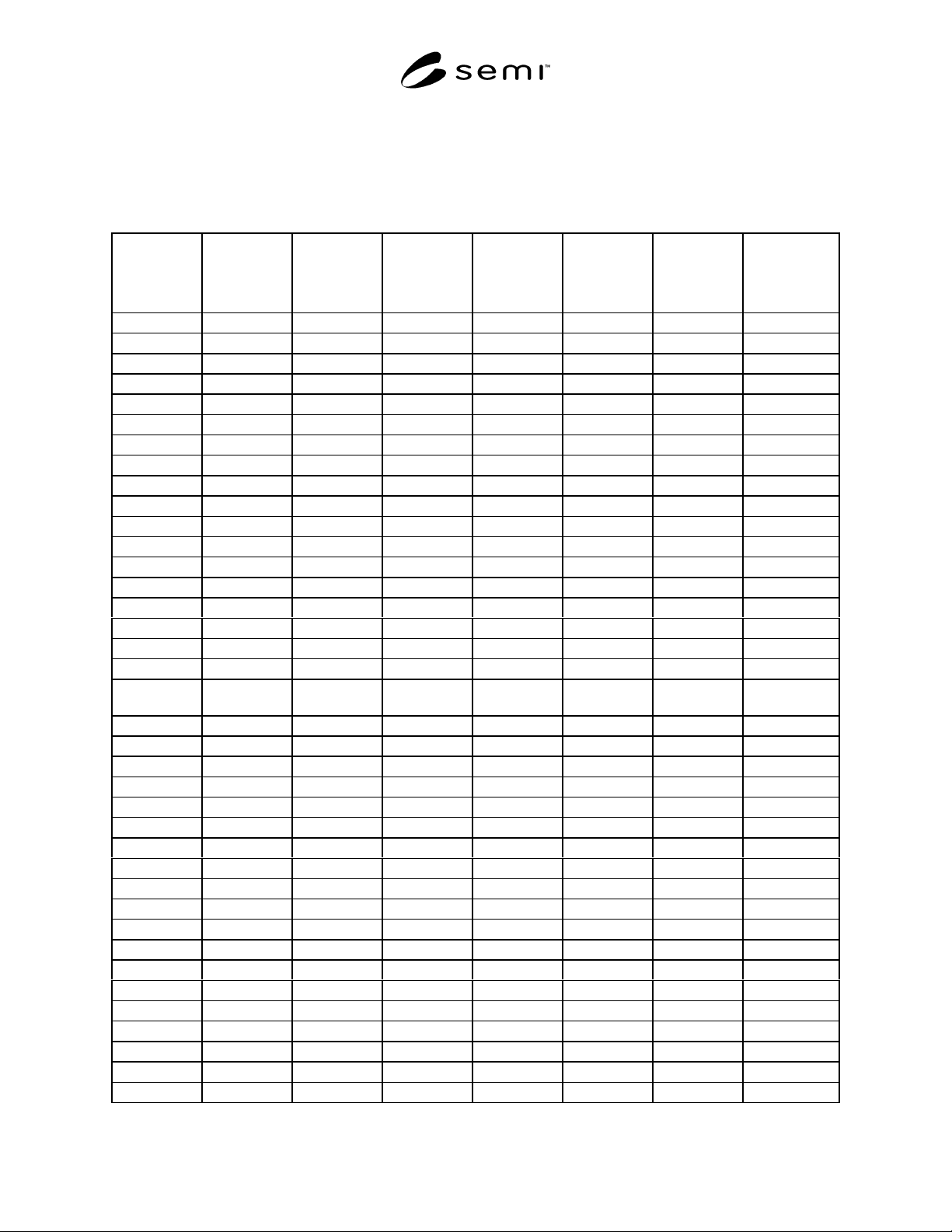
Table 4 Ceramic Cerdip Cap Dimensions and Tolerance Requirements
Description Body Length Body Width
Thickness
Min. Max. Cavity Length Cavity Width
Cavity Depth
(Measured at
Cavity
Bottom) Units
8SSI 0.380 ± 0.004 0.248 ± 0.003 0.050 - 0.055 0.260 ± 0.004 0.157 ± 0.003 0.018 ± 0.003 in
9.65 ± 0.102 6.30 ± 0.076 1.27 - 1.40 6.60 ± 0.102 6.60 ± 0.102 3.99 ± 0.076 mm
8LSI 0.380 ± 0.004 0.288 ± 0.003 0.050 - 0.055 0.260 ± 0.004 0.185 ± 0.003 0.018 ± 0.003 in
9.65 ± 0.012 7.32 ± 0.076 1.27 - 1.40 6.60 ± 0.102 4.70 ± 0.076 0.457 ± 0.076 mm
14/16SSI 0.760 ± 0.007 0.248 ± 0.004 0.050 - 0.055 0.350 ± 0.004 0.157 ± 0.003 0.018 ± 0.003 in
19.30 ± 0.178 6.81 ± 0.076 1.27 - 1.40 8.89 ± 0.102 4.32 ± 0.076 0.457 ± 0.076 mm
16SLI/VLSI 0.760 ± 0.007 0.288 ± 0.003 0.050 - 0.055 0.450 ± 0.005 0.195 ± 0.003 0.018 ± 0.003 in
19.30 ± 0.178 7.32 ± 0.076 1.27 - 1.40 10.67 ± 0.127 4.95 ± 0.076 0.457 ± 0.076 mm
18MSI 0.890 ± 0.008 0.268 ± 0.003 0.050 - 0.055 0.350 ± 0.004 0.170 ± 0.003 0.018 ± 0.003 in
22.61 ± 0.203 6.81 ± 0.076 1.27 - 1.40 8.89 ± 0.102 4.32 ± 0.076 0.457 ± 0.076 mm
18LSI 0.890 ± 0.008 0.288 ± 0.003 0.050 - 0.055 0.350 ± 0.004 0.185 ± 0.003 0.018 ± 0.003 in
22.61 ± 0.203 7.32 ± 0.076 1.27 - 1.40 8.89 ± 0.102 4.70 ± 0.076 0.457 ± 0.076 mm
18VLSI 0.890 ± 0.008 0.288 ± 0.003 0.050 - 0.055 0.420 ± 0.004 0.195 ± 0.003 0.018 ± 0.003 in
22.61 ± 0.203 7.32 ± 0.076 1.27 - 1.40 10.67 ± 0.102 4.95 ± 0.076 0.457 ± 0.076 mm
20MSI 0.950 ± 0.010 0.268 ± 0.003 0.050 ± 0.055 0.300 ± 0.004 0.170 ± 0.003 0.018 ± 0.003 in
24.13 ± 0.254 6.81 ± 0.076 1.27 - 1.40 7.62 ± 0.102 4.32 ± 0.076 4.57 ± 0.076 mm
20LSI/VLSI 0.950 ± 0.010 0.288 ± 0.003 0.050 - 0.055 0.380 ± 0.004 0.190 ± 0.003 0.018 ± 0.003 in
24.13 ± 0.254 7.32 ± 0.076 1.27 - 1.40 9.65 ± 0.102 4.83 ± 0.076 0.457 ± 0.076 mm
22MSI/LSI/VL
SI
1.070 ± 0.010 0.380 ± 0.004 0.050 - 0.055 0.370 ± 0.005 0.275 ± 0.004 0.018 ± 0.003 in
27.17 ± 0.254 9.65 ± 0.102 1.27 - 1.40 9.40 ± 0.127 6.99 ± 0.102 0.457 ± 0.076 mm
24MSI/LSI 1.250 ± 0.010 0.520 ± 0.006 0.050 - 0.055 0.400 ± 0.005 0.330 ± 0.005 0.018 ± 0.003 in
31.75 ± 0.254 13.21 ± 0.152 1.27 - 1.40 10.16 ± 0.127 8.38 ± 0.127 0.457 ± 0.076 mm
24VLSI 1.250 ± 0.010 0.577 ± 0.006 0.050 - 0.056 0.560 ± 0.006 0.380 ± 0.005 0.018 ± 0.003 in
31.75 ± 0.254 14.65 ± 0.152 1.27 - 1.42 14.22 ± 0.152 9.65 ± 0.127 0.457 ± 0.076 mm
24SD3S 1.250 ± 0.010 0.288 ± 0.003 0.050 - 0.055 0.350 ± 0.004 0.190 ± 0.003 0.018 ± 0.003 in
31.75 ± 0.254 7.32 ± 0.076 1.27 - 1.40 8.89 ± 0.102 4.83 ± 0.076 0.457 ± 0.076 mm
24SD3M 1.250 ± 0.010 0.288 ± 0.003 0.050 - 0.055 0.490 ± 0.005 0.195 ± 0.003 0.018 ± 0.003 in
31.75 ± 0.254 7.32 ± 0.076 1.27 - 1.40 12.45 ± 0.127 4.95 ± 0.076 0.457 ± 0.076 mm
24SD4M 1.250 ± 0.010 0.380 ± 0.004 0.050 - 0.055 0.235 ± 0.004 0.235 ± 0.004 0.018 ± 0.003 in
31.75 ± 0.254 9.65 ± 0.102 1.27 - 1.40 5.97 ± 0.102 5.97 ± 0.102 0.457 ± 0.076 mm
28MSI/LSI 1.450 ± 0.010 0.520 ± 0.006 0.050 - 0.055 0.400 ± 0.005 0.330 ± 0.005 0.018 ± 0.003 in
36.83 ± 0.254 13.21 ± 0.152 1.27 - 1.40 10.16 ± 0.127 8.38 ± 0.127 0.457 ± 0.076 mm
28VLSI 1.450 ± 0.010 0.577 ± 0.006 0.050 - 0.056 0.560 ± 0.005 0.380 ± 0.005 0.018 ± 0.003 in
36.83 ± 0.254 14.65 ± 0.152 1.27 - 1.42 14.22 ± 0.127 9.65 ± 0.127 0.457 ± 0.076 mm
40 MSI/LSI 2.050 ± 0.012 0.520 ± 0.006 0.050 - 0.055 0.475 ± 0.005 0.365 ± 0.005 0.018 ± 0.003 in
52.07 ± 0.305 13.21 ± 0.152 1.27 - 1.40 12.07 ± 0.127 9.27 ± 0.127 0.457 ± 0.076 mm
48MSI 2.450 ± 0.015 0.577 ± 0.006 0.050 - 0.056 0.400 ± 0.005 0.400 ± 0.005 0.018 ± 0.003 in
14.65 ± 0.152 14.65 ± 0.152 1.27 - 1.42 10.16 ± 0.127 10.16 ± 0.127 0.457 ± 0.076 mm