semi合集-English.pdf - 第3654页
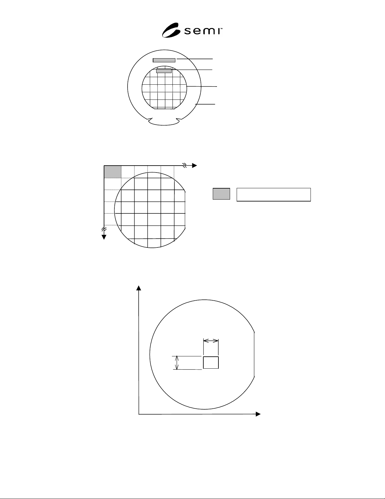
SEMI E142-0705 © SEMI 2005 16 FRAME ID WAF ER ID FILM FRAME WAF E R Figure A1-5 Example of WaferID and FrameID Position OR IGIN Column Row 0 12 3 4 0 1 2 3 4 Map Axis Origin Po sition Figure A1-6 (Ex.) Map Coordinates Sy…
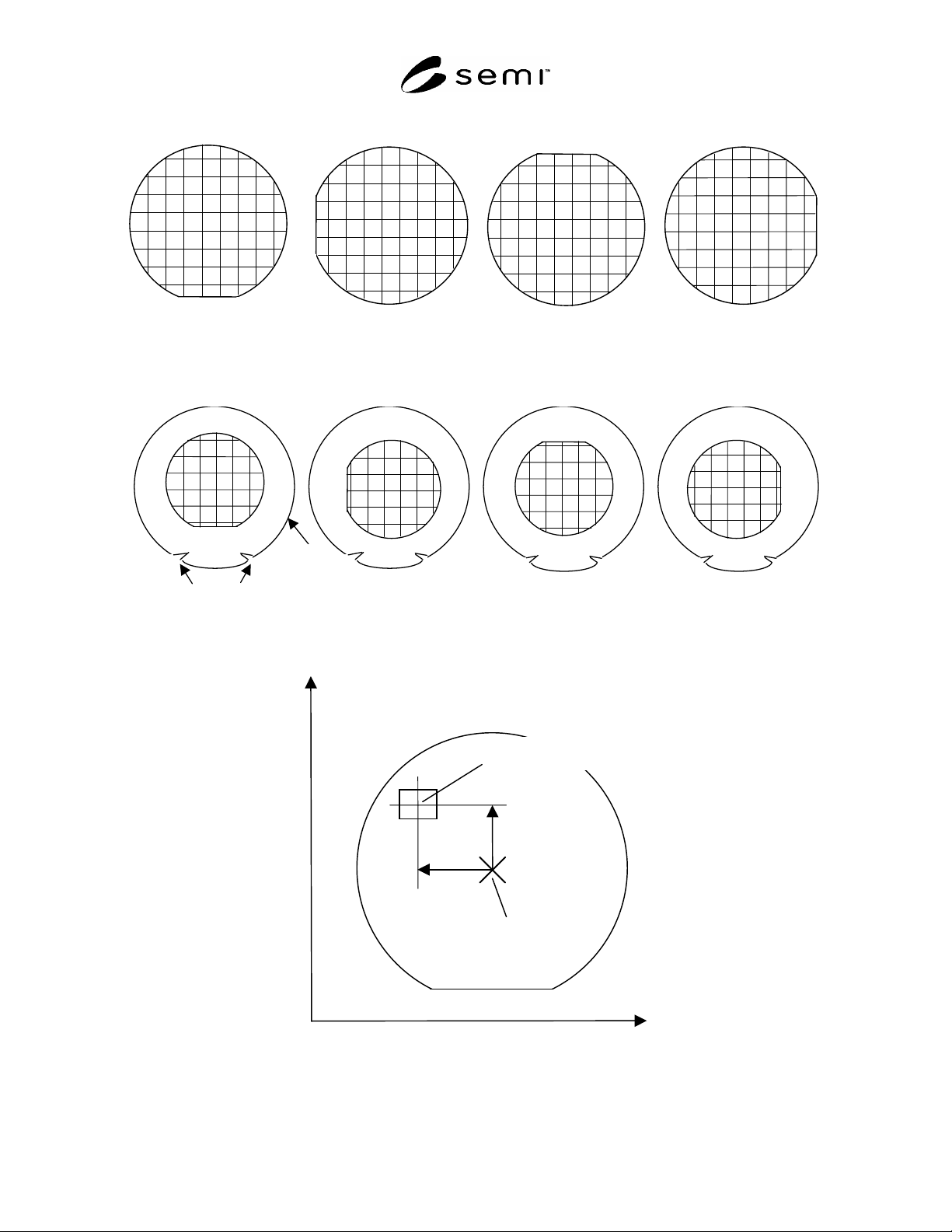
SEMI E142-0705 © SEMI 2005 15
0 deg. 90 deg. 180 deg. 270 deg.
Figure A1-2
Orientation of the Wafer Flat or Notch (Orientation)
FILM
FRAME
NOTCH
0 deg. 90 deg. 180 deg. 270 deg.
Figure A1-3
Orientation of the Wafer Flat or Notch on the Film Frame
+Y
+X
WAFER CENTER
REFERENCE CHIP CENTER
-x
y
Figure A1-4
Reference Device Position
SEMI E142-0705 © SEMI 2005 16
FRAME ID
WAFER ID
FILM FRAME
WAFER
Figure A1-5
Example of WaferID and FrameID Position
ORIGIN
Column
Row
0
1234
0
1
2
3
4
Map Axis Origin Position
Figure A1-6
(Ex.) Map Coordinates System (OriginLocation = Top Left Top Side)
+Y
+X
x
y
Figure A1-7
Device Size Coordinates
SEMI E142-0705 © SEMI 2005 17
0
Y
X
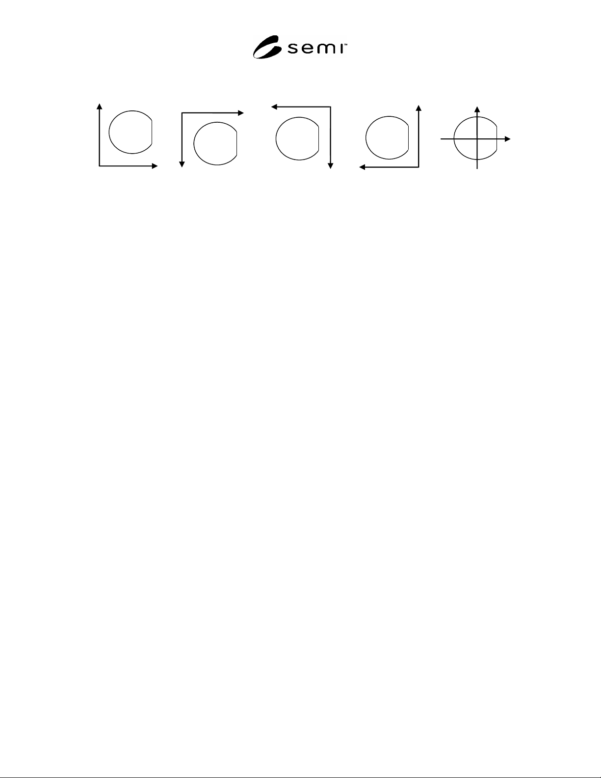
LowerLeft
UpRight
0
Y
X
0
X
Y
0
X
Y
0
X
Y
UpperLeft
DownRight
UpperRight
DownLeft
LowerRight
UpLeft
Center
UpRight
Figure A1-8
Wafer Coordinate to Address Devices (OriginLocation)