semi合集-English.pdf - 第993页
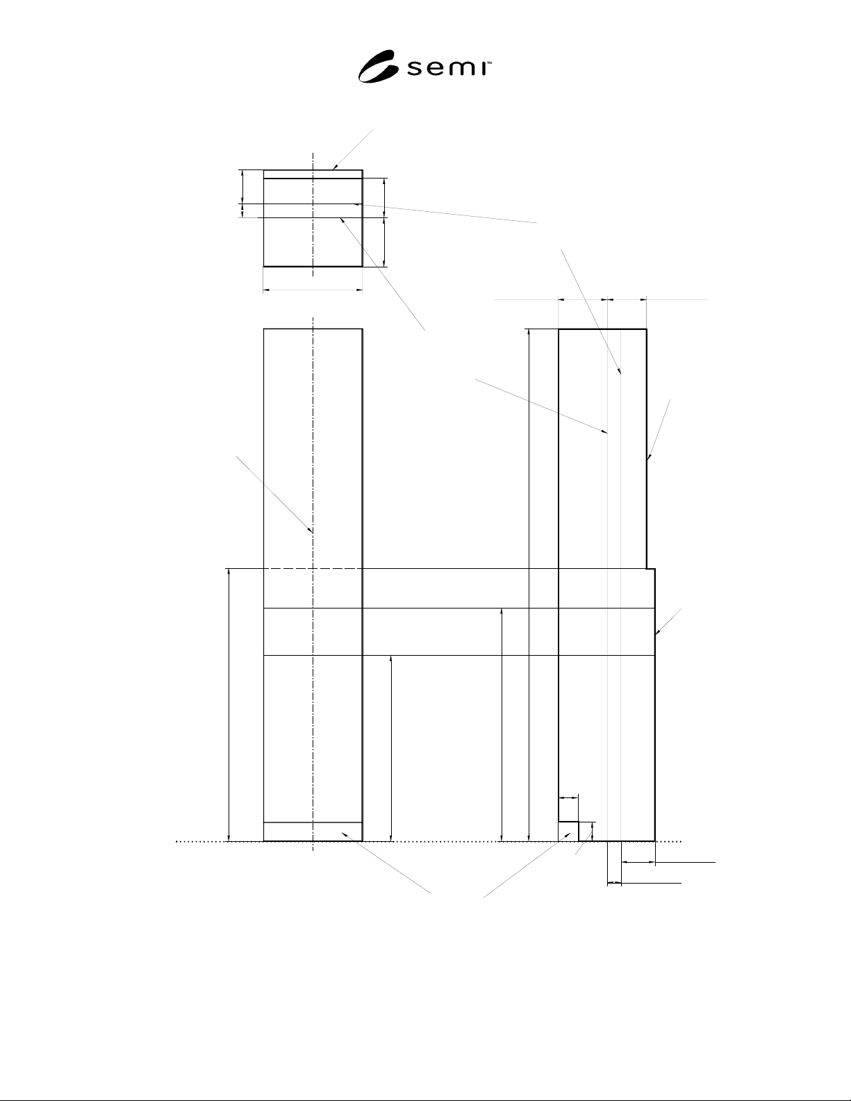
SEMI E131-0304 © SEMI 2004 3 be followed depend ing on the nominal wafer-seatin g plane selected. 6.4 Maximum Outer Dime nsions — If the IMM is intended to be located at the front side of a tool (where load ports are usu…

SEMI E131-0304 © SEMI 2004 2
SEMI E127 — Specification for Integrated
Measurement Module Communications: Concepts,
Behavior, and Services (IMMC)
NOTICE: Unless otherwise indicated, all documents
cited shall be the latest published versions.
5 Terminology
5.1 Abbreviations and Acronyms
5.1.1 IMM — Integrated Measurement Module
5.2 Definitions
5.2.1 bilateral datum plane — a vertical plane that
bisects the substrates and that is perpendicular to both
the horizontal and facial datum planes. (As defined in
SEMI E57.)
5.2.2 BOLTS plane — a plane parallel to the facial
datum plane near the front of the tool where the
box/opener loader is attached. (As defined in SEMI
E63.)
5.2.3 facial datum plane — a vertical plane that bisects
the wafers and that is parallel to the front side of the
carrier (where wafers are removed or inserted). On tool
load ports, it is also parallel to the load face plane
specified in SEMI E15 on the side of the tool where the
carrier is loaded and unloaded. (As defined in SEMI
E57.)
5.2.4 horizontal datum plane — a horizontal plane
from which projects the kinematic-coupling pins on
which the carrier sits. On tool load ports, it is at the
load height specified in SEMI E15 and might not be
physically realized as a surface. (As defined in SEMI
E57.)
5.2.5 integrated measurement module (IMM) — a
measurement module intended to be integrated into
manufacturing equipment, and with the capability of
receiving substrates from the equipment, measuring
those substrates, and returning the substrates and the
measurement results to the equipment and other
concerned clients. (As defined in SEMI E127.)
5.2.6 measurement module — an equipment module
whose intended function is to measure or inspect the
product and to report the results. Measurement of the
product is the factory’s means of gaining feedback on
the manufacturing process. (As defined in SEMI
E127.)
5.2.7 nominal wafer-seating plane — horizontal plane
that bisects the wafer pick-up volume. (As defined in
SEMI E1.9.)
6 Requirements
6.1 The IMM is required to mate with an interface as
defined by SEMI E63. This includes meeting the
requirements for the hole opening, bolt hole pattern,
and other relevant requirements. Note that certain
requirements in SEMI E63, such as y76 (facial datum
plane when carrier is undocked), do not have relevance
for the IMM but will not be in conflict.
6.2 Use of Datum Planes — The location in space
where a substrate is delivered to an IMM is the
intersection of three orthogonal datum planes defined in
other standards: the facial datum plane, the nominal
wafer-seating plane and the bilateral datum plane. The
BOLTS plane, as in SEMI E63, is defined to be parallel
to, and at a distance of y70 from the facial datum plane.
6.2.1 Bilateral Datum Plane — All bilateral
dimensions of the interface are symmetric about the
bilateral datum plane as shown in Figure 1.
6.2.2 Facial Datum Plane — This is the vertical plane,
parallel to the BOLTS plane, which bisects the
substrate at the insertion and removal position of the
substrate inside of the IMM. The distance from the
BOLTS plane to the facial datum plane in the IMM is
determined by y70 of SEMI E63.
6.2.3 Nominal Wafer-Seating Plane — The nominal
wafer-seating plane is the horizontal plane within the
IMM where a substrate is to be loaded to or unloaded
from by the tool. It can be anywhere between the given
minimum and maximum values that follow. This range
is not defined by a single standard, rather it results from
a combination of dimensions of SEMI E1.9, SEMI
E15.1 and SEMI E47.1. (See Figure 1.)
6.2.3.1 The minimum value for a nominal wafer-
seating plane is the sum of (H + z44 + z8), measured
from the floor.
6.2.3.2 The maximum value for a nominal wafer-
seating plane is calculated by (H + z44 + z8 + (25-1) *
z12), measured from the floor.
6.2.3.3 For both calculations, H is from SEMI E15.1,
z44 is from SEMI E47.1, and z8 and z12 are from
SEMI E1.9.
6.3 Internal Clearances — There are requirements
relating to clearances inside the IMM. These relate to
robot arm requirements for substrate handoff, and can
be referenced from SEMI E1.9 and SEMI E47.1 as the
same restrictions apply.
6.3.1 This includes clearance in front of the wafer set-
down location of radius r3, and heights bounded by z11
and z10 relative to the nominal wafer-seating plane.
All clearance requirements above the highest and below
the lowest slot from SEMI E1.9 and SEMI E47.1 must

SEMI E131-0304 © SEMI 2004 3
be followed depending on the nominal wafer-seating
plane selected.
6.4 Maximum Outer Dimensions — If the IMM is
intended to be located at the front side of a tool (where
load ports are usually located), the outer dimensions of
the IMM shall not exceed the volume as it would be
used, when a load port is attached to a BOLTS-M
interface.
6.4.1 Depth — The depth of the IMM located at the
front of the process tool shall not exceed the maximum
depth of a load port. The entire depth of the IMM shall
not exceed the sum of y70 + y76 + D (from SEMI E63
and SEMI E15.1 respectively), as measured from the
BOLTS plane.
6.4.1.1 The IMM shall not extend toward the tool
beyond the BOLTS plane, except for possible
temporary use of the reserved space defined in SEMI
E63.
6.4.2 Width — If locating the IMM adjacent to another
load port, there are width requirements defined by the
carrier centroid spacing dimension S from SEMI E15.1.
6.4.2.1 If locating the IMM adjacent to an occupied
load port containing a FOUP with handles, then the
design of the width should not compromise the C1
clearance dimension from SEMI E15.1.
NOTE 3: Most tools today are designed with the dimension
S chosen for spacing of boxes with handles. If the IMM
width exceeds twice the x50 dimension for a FOUP with
handles (from SEMI E47.1) then the IMM may not comply
with the C1 requirement for integration with most existing
tools.
6.4.3 Height — A height H2 (from SEMI E15.1) is the
upper maximum boundary for the IMM when located at
the front of the tool.
6.4.4 Exclusion Volume — There is an exclusion
volume, defined by dimensions L
d
and L
h
at the bottom
rear of the IMM reserved for requirements from SEMI
E64. The width of this exclusion volume is the full
width of the tool.
6.4.5 The front of the IMM (towards the tool) between
the floor and up to the height of a load port, as given by
the sum of H (SEMI E15.1) plus z79 (SEMI E63), is
identical with the BOLTS plane. Above this height, the
front of the IMM is limited by the equipment boundary
as defined in SEMI E15.1.
NOTE 4: The BOLTS plane and the equipment boundary are
defined by a different set of dimensions and thus are at
different positions. The BOLTS plane is located more
towards the tool.
7 Related Documents
7.1 SEMI Standards
SEMI E6 — Guide for Semiconductor Equipment
Installation Documentation
SEMI E51 — Guide for Typical Facilities Services and
Termination Matrix
SEMI E62 — Specification for 300 mm Front-Opening
Interface Mechanical Standard (FIMS)
SEMI E101 — Provisional Guide for EFEM Functional
Structure Model
SEMI E106 — Provisional Overview Guide to SEMI
Standards for Physical Interfaces and Carriers for 300
mm Wafers
SEMI E131-0304 © SEMI 2004 4
plane
Equipment
Side ViewFront View
L (E64)
Top View
bilateral datum
floor
(E63)
(when carrier is undocked)
facial datum plane
(E63)
and removal)
substrate insertion
(when carrier is docked;
facial datum plane
BOLTS plane
(E63)
C
L
C
L
L
C
(E64)
Exclusion volume
(E64)
h
L
d
(E15.1)
boundary
(E63)
BOLTS plane
H2 (E15.1)
wafer-seating plane:
nominal
upper limit for
wafer-seating plane:
nominal
lower limit for
+(25-1)*z12 (E1.9)
+z8 (E1.9)
+z44 (E47.1)
H (E15.1)
+z8 (E1.9)
+z44 (E47.1)
H (E15.1)
+z79 (E63)
H (E15.1)
D (E15.1)
D1 (E15.1)
y76 (E63)
y70 (E63)
y70 (E63)
y76 (E63)
S (E15.1)
D (E15.1) D1 (E15.1)
Figure 1
IMM Dimensional Requirements