semi合集-English.pdf - 第6495页
SEMI G80-0200 © SE MI 2000 3 • Drive Z-State Tests • Multiple Period T ests 6.3.1.2 Level 2 Exter nal Measurement s • Inefficient w /o Auto m ation • Focused S cope • Good Error Observ ability • Drive ( inp ut) T iming T…

SEMI G80-0200 © SEMI 2000 2
4 Referenced Standards
4.1 SEMI Standard
SEMI G79 –– Specification for Overall Digital Timing
Accuracy
5 Terminology
5.1 Abbreviations and Acronyms
5.1.1 1
1
— tester output driver high level
5.1.2 0
2
— tester output driver low level
5.1.3 ATE — automated test equipment
5.1.4 DUT — device under test
5.1.5 H
3
— tester input comparator expect high level.
5.1.6 L
4
— tester input comparator expect low level.
5.1.7 n — highest pin/channel number, and Pin 1 ––
refers to the lowest pin/channel number.
5.1.8 NR — non-return signal format
5.1.9 RTO — return to one signal format.
5.1.10 RTZ — return to zero signal format.
5.1.11 SBC — surround by complement signal format.
5.1.12 Z — tester output driver high i mpedance (“off”)
state.
5.2 Definitions
5.2.1 device insertion errors — error influenced by
device-input capacitance and/or terminations.
5.2.2 edge — time delay created by an ATE delay
generation resource.
5.2.3 high bandwidth oscilloscope — digital sampling
oscilloscope with > 10 GHz bandwidth, using probes
with > 1 GHz bandwidth, 500 ohm input impedance,
2.5pF ± 0.5pF input capacitance and < 0.125" ground
lead.
5.2.4 pin — tester channel
5.2.5 performance board — printed circuit board used
to interface the tester channels to the device under test.
5.2.6 test fixturing errors — error influenced by mis-
matched signal path lengths, impedance discontinuities,
lumped capacitance/inductance elements, and high
frequency loss due to skin effect or interconnects.
1 This convention is not universal. Sometimes a “H” is used.
2 This convention is not universal. Sometimes a “L” is used
3 This convention is not universal. Sometimes a “1” is used.
4 This convention is not universal. Sometimes a “0” is used.
5.2.7 window compare — monitor device contin-
uously during a time interval.
5.2.8 zero_reference_measurement — oscilloscope
measurement of the midpoint of a 0–3v NR signal
rising edge with delay = 0s. This is an arbitrary
reference signal selected by the user of this method.
The method user is free to choose a convenient
reference signal that will allow consistent use of that
signal for making edge placement timing measurements
during tests described in level 2 of this procedure.
6 Summary of Method
6.1 This procedure provides a hierarchical, generic
method of analyzing ATE timing accuracy. The
hierarchy supports two levels of specification analysis.
Broad, composite net results are available by using the
ATE for self-analysis in Level 1.
6.2 At this level, a large amount of data can be effi-
ciently collected, representing the net conformance to
overall timing accuracy specifications. This technique,
however, precludes isolation and detailed analysis of
specific accuracy components. Therefore, a second
level of analysis, incorporating external instruments is
included. While the first level provides efficient, broad
analysis, the second level provides less efficient,
detailed analysis.
6.3 Results from the analyses are saved in a standard
format to facilitate further use for application specific
data reduction. The minimum format is:
test #, channel #, min value, max value
6.3.1 Verification Procedure Summary
6.3.1.1 Level 1 ATE Self-Analysis
• Highly Efficient
• Broad Scope
• Moderate Error Observability
• Drive Input to Compare Output Tests
• 3 Voltages
• 2 Pin Directions
• 503 Test Cycles
5
• 503 Pulse Widths
• 12 Transitions
6
•
4 Formats
• Extended Delay Tests
5 Reference Figure 3.
6 Reference Figure 2.

SEMI G80-0200 © SEMI 20003
• Drive Z-State Tests
• Multiple Period Tests
6.3.1.2 Level 2 External Measurements
• Inefficient w/o Automation
• Focused Scope
• Good Error Observability
• Drive (input) Timing Test
• Compare (output) Timing Test
• Driver Rise Time Test
• Drive (input) Timing Cycle Jitter Test
• High Speed Clock Test
7 Requirements
7.1 Acceptance Tests — Before initiating the test
process, the ATE under evaluation is to be certified by
a representative of the manufacturer or end-user to be
fully operational.
7.2 Personnel Qualification — The individual(s)
operating the ATE under evaluation must be certified or
otherwise qualified to operate this equipment, and be
familiar with the procedures for performing the analysis
called-out in this document.
7.3 Supplemental Equipment — The following equip-
ment is required: A digital sampling oscilloscope with
> 10 GHz bandwidth, probes with > 1 GHz bandwidth,
500 ohm input impedance, 2.5 pF ± 0.5pF input
capacitance, and < 0.125" ground lead. It is important
that this equipment requirement step be met. Tolerances
called-out in various steps of this procedure were
chosen to be consistent with the general equipment
specified in this equipment specification requirement.
7.4 This Procedure — It is highly recommended that
the user of this method read this document (SEMI G80)
in its entirety.
7.5 System — Test system usage will be available on
a continuous basis and uninterrupted during the allotted
time needed to perform this timing analysis procedure.
7.6 Application Program — It is required that an
application program be written to perform the steps
called-out in this procedure. That program will act as a
means of reliable and consistent interaction between the
tester and supplemental equipment. In so executing,
that program will also facilitate the data collection
process that will ultimately lead to the timing analysis
conclusions this procedure produces.
7.7 The Method — The recommended procedure, con-
tained primarily in Section 10 of this document, is gen-
erically written and will serve as a guide in producing
the required program, written in the test application
software language of the system under evaluation.
7.8 ATE System Performance (Load) Boards — To
collect data two performance/load boards will be
required. For one of these performance boards it is
recommended that adjacent tester channels be shorted
together with minimum and equal length intercon-
nections. This board will facilitate the data collection
process for Level 1 and in part for Level 2. The second
board is to have an open driver to comparator
connection and will be used for Level 2 drive input
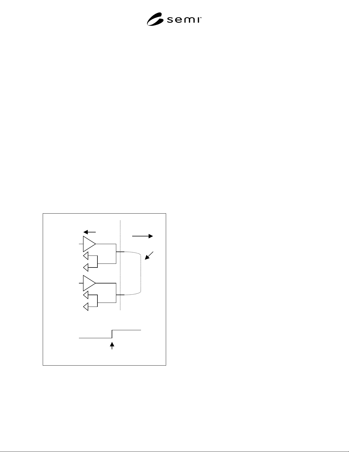
timing tests. Reference Figures 1 and 4.
7.9 Exceptions — It is expected that the user of this
method execute the procedures as described in this
document. If the method user should choose to deviate
from the procedures recommended in this document it
is expected that an appropriate description of that
deviation be entered in the EXCEPTIONS PAGE
provided in Appendix 3.
8 Test Conditions
8.1 Environmental — It is a requirement that the
procedure called-out in this document be executed
within the intended environmental operating conditions
specified by the equipment supplier. Operating
temperature requirements specified by the equipment
supplier must be maintained.
8.2 Optional Execution — The user of this procedure
may consider rerunning this procedure at environmental
(temperature) extremes other than nominal.
8.3 Warm-up Period — It is essential that all
equipment used or under evaluation be allowed to
warm-up in accordance with the manufacturer’s
specified requirements for equipment stabilization.
8.4 Optional Data Collection — Data may be taken
immediately after equipment calibration. However, the
user of this procedure may wish to take additional data
at subsequent time intervals, but within the known good
calibration window for the system under evaluation.
9 Preparation of Apparatus
9.1 Equipment Configuration — The equipment under
evaluation must be configured for its normal and
intended operation. No special considerations such as
additional cooling or removal of equipment skins are to
be undertaken.
9.2 Equipment Calibration — The equipment under
evaluation must be fully calibrated before this proce-
dure is executed. No special calibration is to be
SEMI G80-0200 © SEMI 2000 4
performed and the equipment is to be configured for
normal and intended operation.
9.3 Supplemental Equipment Calibration — External
equipment used for level 2 data collection in this
procedure must be verified for proper calibration.
10 Test Method Procedure
10.1 The procedure is comprised of Level 1 tests and
Level 2 tests. Any ATE capability described in the
following tests that is not available on the ATE under
analysis is not required for compliance to the
procedure, but should be noted in the verification
results Table 1 and Table 2.
10.2 Each test system is different; thus this procedure
is generic. Regardless, it will provide comprehensive
results when the specific application is created using
this procedure as a guide. Per the requirements, a load
board and application program written to accommodate
the procedure should be in place when the procedure is
executed. This procedure is to be executed per the
requirements outlined in Section 7 of this document.
When these requirements are met, the following steps
will comprise the step by step process for execution of
this Test Method:
Adjacent pins shorted together
Pin n
Pin n+1
Short
Pin n
Driver
Receiver
Pin n+1
Driver
Receiver
Tester
Performance
b
oard
Pairs of adjacent tester pins are shorted together with
a
minimum length interconnect on the performance board.
Figure 1
Level 1 Verification
1. Install the performance board.
2. Power up the system and supplemental equipment,
allow adequate time for stabilization.
3. Load the appropriate application program that
represents the embodiment of the procedure called out
in Sections 10.3.1, 10.3.4, 10.3.5, and 10.3.6 for Level
1 as well as Sections 10.4.1, 10.4.2, 10.4.3, 10.4.4,
10.4.5, and 10.4.6 for Level 2.
4. Execute the method to completion. The application
program can capture the data for Level 1 and Level 2
and store that for later analysis.
5. This procedure calls for various time measurements
to be made at specified voltage points or signal levels.
The user is encouraged to maintain these values to keep
the method results constants when system to system
comparisons are being made. Regardless, he is free to
adjust these measurement points or levels to accommo-
date specific integrated circuit technology requirements
important to that product and the system being
analyzed. When that occurs documentation of those
procedure variations must be entered in Appendix 3
(Exceptions Page).
6. Best results from this procedure are achieved if a
consistent measurement methodology is maintained.
This is important when making time measurements
relative to a particular transition point on a signal edge.
This method recommends that when signal measure-
ments are specified at a particular transition point, i.e.,
50%, that this point on the edge be determined relative
to the 0% or 100% steady state levels displayed on the
oscilloscope, after any aberrations due to the transition
have expired. A tester reference channel, the lowest
channel, should be used to set the measurement point(s)
and then consistently used as the basis for subsequent
measurements for the remaining tester channels.
7. Data Analysis –– Analyze the captured data and
make the appropriate data entries to Table 1, provided
in this method document.
8. When this method execution is complete, document
all method exceptions in the EXCEPTIONS section of
this document (Appendix 3).
9. Results –– Data entry to Table 2. Make the
appropriate data entries to Table 2, provided in this
method document and supplemented with examples
contained in Appendix 2.
10.2.1 Level 1 requires no external equipment for
completion, whereas Level 2 does require use of
external equipment. The user is free to implement this
procedure through total manual intervention. On the
other hand, the user may choose to apply an automated
or robotic approach to data collection for Level 2.
Regardless, the user is advised that tester and external