semi合集-English.pdf - 第426页
SEMI E57-0305 © SEMI 1996, 2005 2 4.1.4 facial datum pl ane — a vertical plane that bisects the wafers and th at is parallel to the fron t side of the carrier (where wafers are rem oved or inserted). On tool load ports, …

SEMI E57-0305 © SEMI 1996, 2005 1
SEMI E57-0600 (Reapproved 0305)
MECHANICAL SPECIFICATION FOR KINEMATIC COUPLINGS USED
TO ALIGN AND SUPPORT 300 mm WAFER CARRIERS
This specification was technically reapproved by the Global Physical Interfaces and Carriers Committee and
is the direct responsibility of the North American Physical Interfaces and Carriers Committee. Current
edition approved by the North American Regional Standards Committee on November 4, 2004. Initially
available at www.semi.org January 2005; to be published March 2005. Originally published in 1996;
previously published June 2000.
1 Purpose
1.1 This standard specifies the mechanical couplings used to ergonomically align and precisely support 300 mm
wafer carriers (including transport cassettes, process cassettes, quartz boats, pods, lot boxes, and shipping boxes).
Such a kinematic coupling can be used at several interfaces, including:
between a box or cassette and a tool load-port or vehicle nest,
between a transport cassette and a box, and
between a process cassette or quartz boat and the floor of a process chamber.
2 Scope
2.1 This standard is intended to set an appropriate level of specification that places minimal limits on innovation
while ensuring modularity and inter-changeability at all mechanical interfaces. Only the bottom half of the
kinematic coupling is specified so that suppliers can be flexible in designing wafer carriers that can mate with it.
NOTICE: This standard does not purport to address safety issues, if any, associated with its use. It is the
responsibility of the users of this standard to establish appropriate safety and health practices and determine the
applicability of regulatory or other limitations prior to use.
3 Referenced Standards
3.1 SEMI Standards
SEMI E15 — Specification for Tool Load Port
SEMI E19 — Standard Mechanical Interface (SMIF)
SEMI E19.4 — 200 mm Standard Mechanical Interface (SMIF)
3.2 ISO Document
1
ISO 4287 — Geometrical Product Specifications (GPS) — Surface texture: Profile method — Terms, definitions
and surface texture parameters
NOTICE: Unless otherwise indicated, all documents cited shall be the latest published versions.
4 Terminology
4.1 Definitions
4.1.1 bilateral datum plane — a vertical plane that bisects the wafers and that is perpendicular to both the
horizontal and facial datum planes.
4.1.2 box — a protective portable container for a cassette and/or substrate(s).
4.1.3 cassette — a open structure that holds one or more substrates.
1 International Organization for Standardization, ISO Central Secretariat, 1, rue de Varembé, Case postale 56, CH-1211 Geneva 20, Switzerland.
Telephone: 41.22.749.01.11; Fax: 41.22.733.34.30, Website: /www.iso.ch

SEMI E57-0305 © SEMI 1996, 2005 2
4.1.4 facial datum plane — a vertical plane that bisects the wafers and that is parallel to the front side of the carrier
(where wafers are removed or inserted). On tool load ports, it is also parallel to the load face plane specified in
SEMI E15 on the side of the tool where the carrier is loaded and unloaded.
4.1.5 horizontal datum plane — a horizontal plane from which projects the kinematic-coupling pins on which the
carrier sits. On tool load ports, it is at the load height specified in SEMI E15 and might not be physically realized as
a surface.
4.1.6 nominal wafer center line — the line that is defined by the intersection of the two vertical datum planes (facial
and bilateral) and that passes through the nominal centers of the seated wafers (which must be horizontal when the
carrier is placed on the coupling).
4.1.7 pod — a box having a Standard Mechanical Interface (SMIF) per SEMI E19.
4.1.8 wafer carrier — any cassette, box, pod, or boat that contains wafers (as defined in SEMI E15).
5 Requirements
5.1 Kinematic Coupling Pin Shapes — The physical alignment interface on the bottom of the wafer carrier consists
of features (not specified in this standard) that mate with six pins underneath. As shown in Figure 1 and defined in
Table 1, each pin is radially symmetric about the vertical center axis line and can be seen as the intersection of a
cylinder of diameter d91 and a sphere of radius r93 (which might contact a flat plate). An additional rounding radius
r95 provides contact with angled mating surfaces, and blend radii r94 and r96 smooth the resulting edges. The final
roughness height of the over-all surface finish must be less than or equal to r97. Dimensions r92 and z91 have zero
tolerance because they only give a distance to another toleranced dimension. (Dimensions in parenthesis are not part
of the requirements in this standard but are intended to clarify the preparation of manufacturing instructions.)
5.2 Kinematic Coupling Pin Locations — The pins are arranged in three sets with two pins in each set. As shown in
Figure 2, the outer pin in each set is designated the primary pin for use on a tool load-port or vehicle nest or inside a
box, and the inner pin in each set is designated the secondary pin for use on a robotic arm that would pick up the
carrier (typically from the side opposite the load face plane). The location of each pin is determined with respect to
the three orthogonal datum planes defined in §4: the horizontal datum plane, the facial datum plane, and the bilateral
datum plane. Figure 3 shows the locations of the kinematic coupling pins as viewed from above, and Table 2 defines
the locations (all of which are bilaterally symmetric about the bilateral datum plane). Angle is shown in Figure 3
for clarity and is not part of the requirements in this standard.
5.3 Empirical Determination of Datum Plane Locations — Given a set of three primary or secondary kinematic
coupling pins, the datum planes should be determined as follows. The two pins that are closest together are the front
pins which (along with a known vertical direction) define a Cartesian coordinate system. The center axis line of each
pin is defined to be the vertical line whose x
(left-right) coordinate is the average of the maximum protrusions of the
pin to the left and to the right and whose y (front-back) coordinate is the average of the maximum protrusions of the
pin to the front and to the back. The bilateral datum plane is defined to be the vertical plane that contains the center
axis line of the rear pin and that is equally distant from the center axis lines of the front pins. The facial datum plane
is defined to be the vertical plane that is perpendicular to the bilateral datum plane and whose distance to the center
axis line of the rear pin is 1.5 times the average of the distances to the center axis lines of the front pins. The
horizontal datum plane is defined to be the horizontal plane that is 13 mm (0.51 in.) below the average of the heights
of the highest and lowest pin tops. Once these datum planes have been determined, the three kinematic coupling pins
can be evaluated to see if they conform to ¶¶5.1 and 5.2 of this specification. If they comply, the kinematic coupling
pins and datum planes can be used to evaluate the compliance of carriers to standards cited in §6.
6 Related Documents
6.1 SEMI Standards
SEMI E1.9 — Mechanical Specification for Cassettes Used to Transport and Store 300 mm Wafers
SEMI E47.1 — Provisional Mechanical Specification for Boxes and Pods Used to Transport and Store 300 mm
Wafers
SEMI E62 — Provisional Specification for 300 mm Front-Opening Interface Mechanical Standard (FIMS)
SEMI E63 — Mechanical Specification for 300 mm Box Opener/Loader to Tool Standard (BOLTS-M) Interface
SEMI E57-0305 © SEMI 1996, 2005 3
SEMI M31 — Provisional Mechanical Specification for Front-Opening Shipping Box Used to Transport and Ship
300 mm Wafers
6.2 Other Documents
Alexander H. Slocum, Precision Machine Design, Society of Manufacturing Engineers, Item Code 2597, 1992
(originally published by Prentice-Hall, 1992)
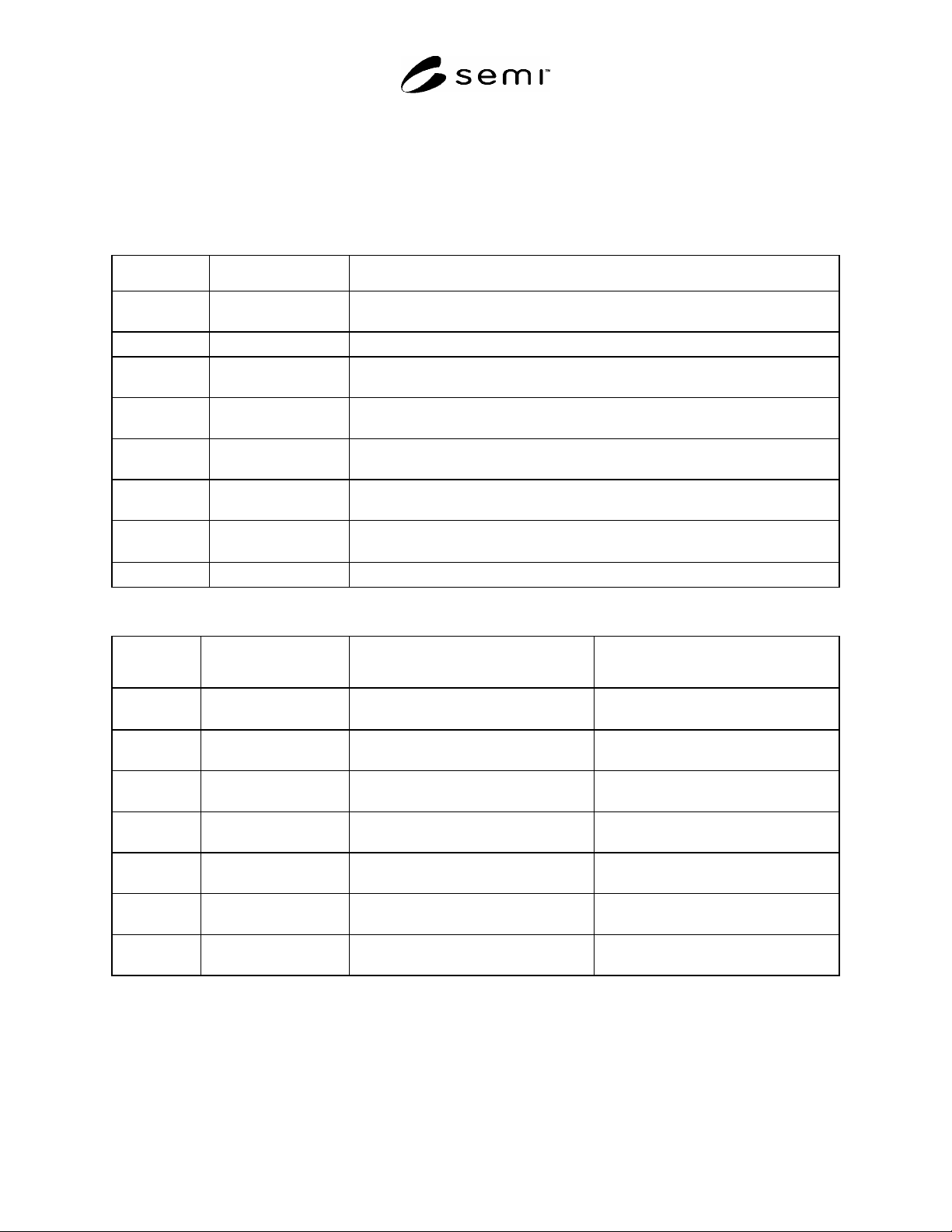
Table 1 Kinematic Coupling Pin Dimensions
Symbol Used Value Specified Dimension Description
d91 12 ± 0.05 mm
(0.4724 ± 0.002 in.)
Diameter of pin centered on the center axis line.
r92 6 mm (0.2362 in.) Radial distance from the center axis line to the origin of the shoulder radius r95.
r93 15 ± 0.05 mm
(0.5906 ± 0.002 in.)
Radial distance from the intersection of the center axis line and z91 to the top of the
pin.
r94 2 ± 0.1 mm
(0.0787 ± 0.004 in.)
Blend radius for the intersection of r93 and r95.
r95 15 ± 0.05 mm
(0.5906 ± 0.002 in.)
Radial distance from the intersection of the horizontal datum plane and r92 to the far
shoulder of the pin.
r96 2 ± 0.1 mm
(0.0787 ± 0.004 in.)
Blend radius for the intersection of r95 and d91.
r97
0.30 m (12 in.)
maximum
Roughness (R
a
) as defined in ISO 4287.
z91 2 mm (0.08 in.) Vertical distance from the horizontal datum plane to the origin of top radius r93.
Table 2 Distances to the Center Axis Lines of the Coupling Pins
Symbol Used Value Specified Datum Plane
Measured from
Pin Center Axis Line(s)
Measured to
r97
0.30 m (12 in.)
maximum
Roughness (R
a
) as defined in ISO 4287 r97
x91 115 ± 0.05 mm
(4.5276 ± 0.002 in.)
bilateral front right and left
primary
x92 92 ± 0.05 mm
(3.6220 ± 0.002 in.)
bilateral front right and left
secondary
y91 80 ± 0.05 mm
(3.1496 ± 0.002 in.)
facial front right and left
primary
y92 120 ± 0.05 mm
(4.7244 ± 0.002 in.)
facial rear
primary
y93 64 ± 0.05 mm
(2.5197 ± 0.002 in.)
facial front right and left
secondary
y94 96 ± 0.05 mm
(3.7795 ± 0.002 in.)
facial rear
secondary