semi合集-English.pdf - 第169页
SEMI E21.1-1296 © SEMI 1992, 2002 1 SEMI E21.1-1296 (Reapproved 1102) CLUSTER TOOL MODULE IN TERFACE 300 mm: MECHANICAL INTERFACE AND WAFER TRANSPORT STANDARD This standard was technically rea pproved by the Global Physi…

SEMI E21-94 © SEMI 1991, 2002 8
R1-8 Clamping
R1-8.1 The standard (see Section 4.3.1) allows a
universal clamping scheme to be employed. Claw
clamps designed for use with ISO flanges are
accommodated by the use of a perimeter groove around
the flange.
R1-8.2 The clamping scheme provides several benefits:
• Independence from any hole pattern requirements.
• Flanges may be connected to flat plates or to other
flanges.
• The number of clamps and the number of sides
used to draw the flanges together may be varied as
required by the compression forces necessary for
the sealing method used. For example, clamps may
be spaced on 30 mm (1.191 in.) centers for metal
seals and on 150 mm (6 in.) centers for elastomeric
seals.
• Any type of clamp may be used that accommodates
the perimeter groove.
NOTICE: SEMI makes no warranties or
representations as to the suitability of the standards set
forth herein for any particular application. The
determination of the suitability of the standard is solely
the responsibility of the user. Users are cautioned to
refer to manufacturer' s instructions, product labels,
product data sheets, and other relevant literature,
respecting any materials or equipment mentioned
herein. These standards are subject to change without
notice.
By publication of this standard, Semiconductor
Equipment and Materials International (SEMI) takes no
position respecting the validity of any patent rights or
copyrights asserted in connection with any items
mentioned in this standard. Users of this standard are
expressly advised that determination of any such patent
rights or copyrights, and the risk of infringement of
such rights are entirely their own responsibility.
Copyright by SEMI® (Semiconductor Equipment and Materials
International), 3081 Zanker Road, San Jose, CA 95134. Reproduction o
f
the contents in whole or in part is forbidden without express written
consent of SEMI.
SEMI E21.1-1296 © SEMI 1992, 2002 1
SEMI E21.1-1296 (Reapproved 1102)
CLUSTER TOOL MODULE INTERFACE 300 mm: MECHANICAL
INTERFACE AND WAFER TRANSPORT STANDARD
This standard was technically reapproved by the Global Physical Interfaces & Carriers Committee and is the
direct responsibility of the North American Physical Interfaces & Carriers Committee. Current edition
reapproved by the North American Regional Standards Committee on July 21, 2002. Initially available at
www.semi.org October 2002; to be published November 2002. Originally published in 1992; previously
published December 1996.
1 Introduction
1.1 The standard provides the requirements to extend
the limits of SEMI E21 from 200 mm diameter wafers
or smaller to 300 mm diameter wafers or smaller.
2 Referenced Standards
2.1 SEMI Standards
SEMI E21 — Cluster Tool Module Interface:
Mechanical Interface and Wafer Transport Standard
3 Requirements
3.1 The standard is identical to E21 (see Related
Infornation R1-1) except for the requirements listed in
Table 1 and Figures 1 and 2.
Table 1 Mechanical Interface Requirements for 300
mm Diameter Wafers
E21
Requirements
300 mm Wafer
Requirements
Transport Maximum
Reach
1
305.0 mm
(12.01 in.)
380.0 mm
(14.96 in.)
Inside Boundary Width-
Interface Seal Zone
2
236.0 mm (9.29
in.)
336.0 mm
(13.23 in.)
Outside Boundary Width-
Interface Seal Zone
2
266.0 mm
(10.47 in.)
366.0 mm
(14.41 in.)
Wafer Transfer Zone
Minimum Width
2
222.0 mm
(8.74 in.)
322.0 mm
(12.68 in.)
Alignment Pins Centerline
Separation
2
300.0 mm
(11.81 in.)
400.0 mm
(15.75 in.)
Flange Width
2
340.0 mm
(13.39 in.)
440.0 mm
(17.32 in.)
Vertical Slot Opening
(Inner boundary of Seal
Zone)
46 mm
(1.811 in.)
Maximum
50 mm
(1.969 in.)
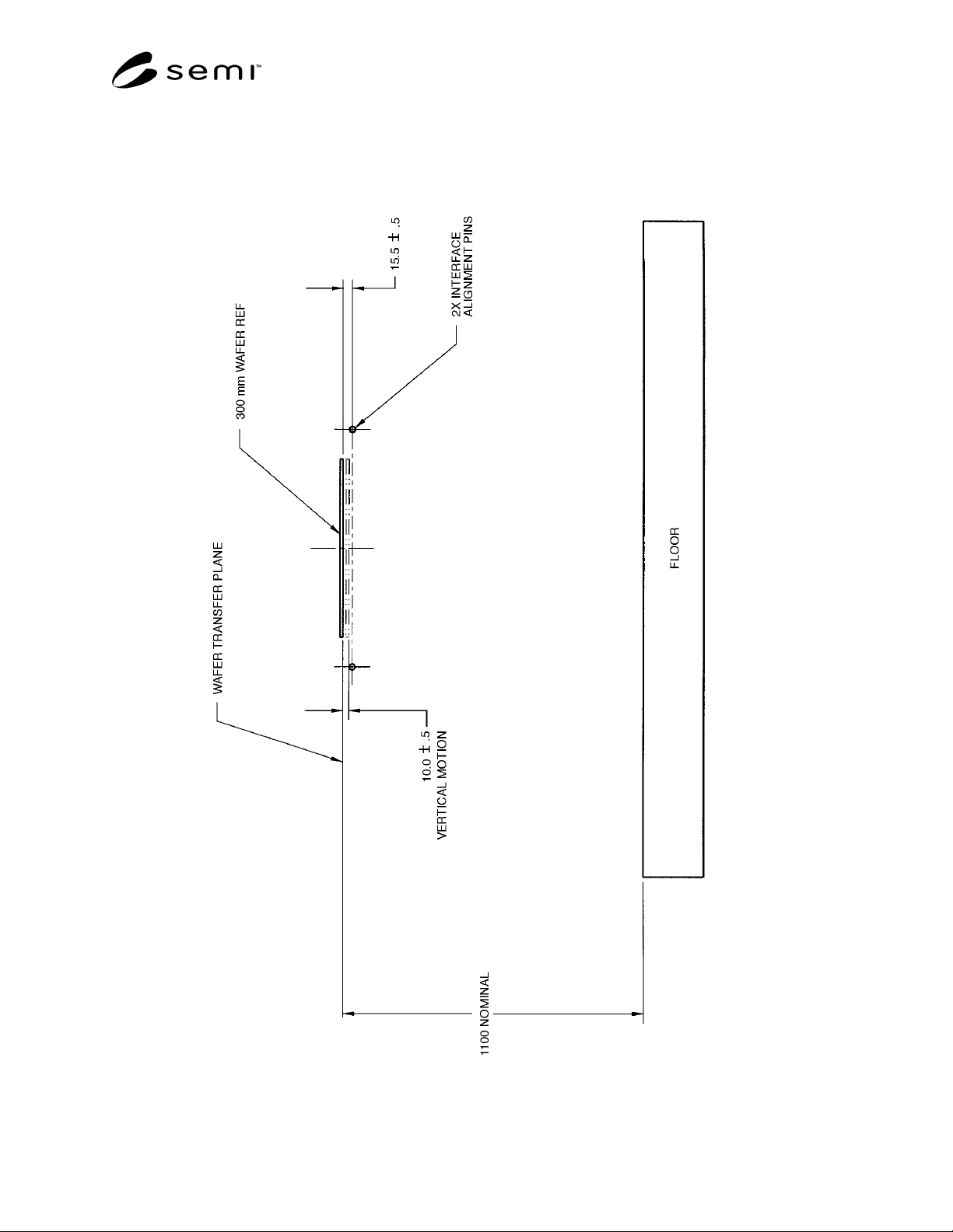
Distance of Wafer Transfer
Plane above Alignment Pin
Datum Line (see Figure 1)
9.5 ± 0.5 mm
(0.37 ± 0.02 in.)
15.5 ± 0.5 mm
(0.61 ± 0.02 in.)
Vertical Motion Capability
(see Figure 1)
6 ± 0.5 mm
(0.24 ± 0.02 in.)
10 ± 0.5 mm
(0.39 ± 0.02 in.)
Minimum Distance of Slot
Top above Alignment Pin
Datum on Attached
Modules
(13 mm) 23 mm
(0.906 in.)
Minimum Distance of Slot
Bottom below Alignment
Pin Datum on Attached
Modules
(13 mm) 13 mm
(0.512 in.)
1. See Related Information R1-2.
2. See Related Information R1-3.
SEMI E21.1-1296 © SEMI 1992, 2002 2
Figure 1
Proposed 300 mm Wafer Transport Plane Elevation