semi合集-English.pdf - 第6119页
SEMI G24-89 © SEMI 198 4, 1996 2 3.7 Place th e probes down on t he l e a d s to be measured. This sh ould be a vertical m ovement only. 3.8 Take th e capacitance reading. I f usi ng auto- zeroing equi pment, this capaci…
SEMI G24-89 © SEMI 1984, 19961
SEMI G24-89
TEST METHOD FOR MEASURING THE LEAD-TO-LEAD AND LOADING
CAPACITANCE OF PACKAGE LEADS
1
1 This test method applies to measurements in the range of 1 to 100 pico farands.
1 Purpose
This document defines the equipment, materials, and
procedures used to measure the lead-to-lead and
loading capacitance of package leads. Semiconductor
packages are shown as examples; however, other
packaging elements can be measured by this method.
2 Equipment and Materials
2.1 Capacitance meter which uses a two probe plus
guard method with two coax cables, or a meter which
utilizes a four probe plus guard method. The four probe
method requires four cables to be modified to connect
to two probes at the probe end of the cables. Both
methods require an 18 awg. or larger insulated wire for
the guard connection. Keep cables at minimum length
(1 meter) unless specified by individual equipment.
Coaxial cables must be used to connect the probes to
the meter. Meter accuracy ± 2%. The probe shields
must be connected together. This connection should be
short, approximately one to two inches.
2.2 Probe station with two coax probes and one
regular probe. Recommendation: Micromanipulator,
two (2) each coax probe model 44-FPC-6000 with #5
collet, and one each OON-FPC-6000 with #3 collet, or
equivalent.
3 Procedure: Lead-to-Lead Capacitance(See
Figure 1)
3.1 Set the instrument to measure at 1 Mhz. If the
equipment has a cable length selection switch, adjust
the switch to the appropriate coax cable length.
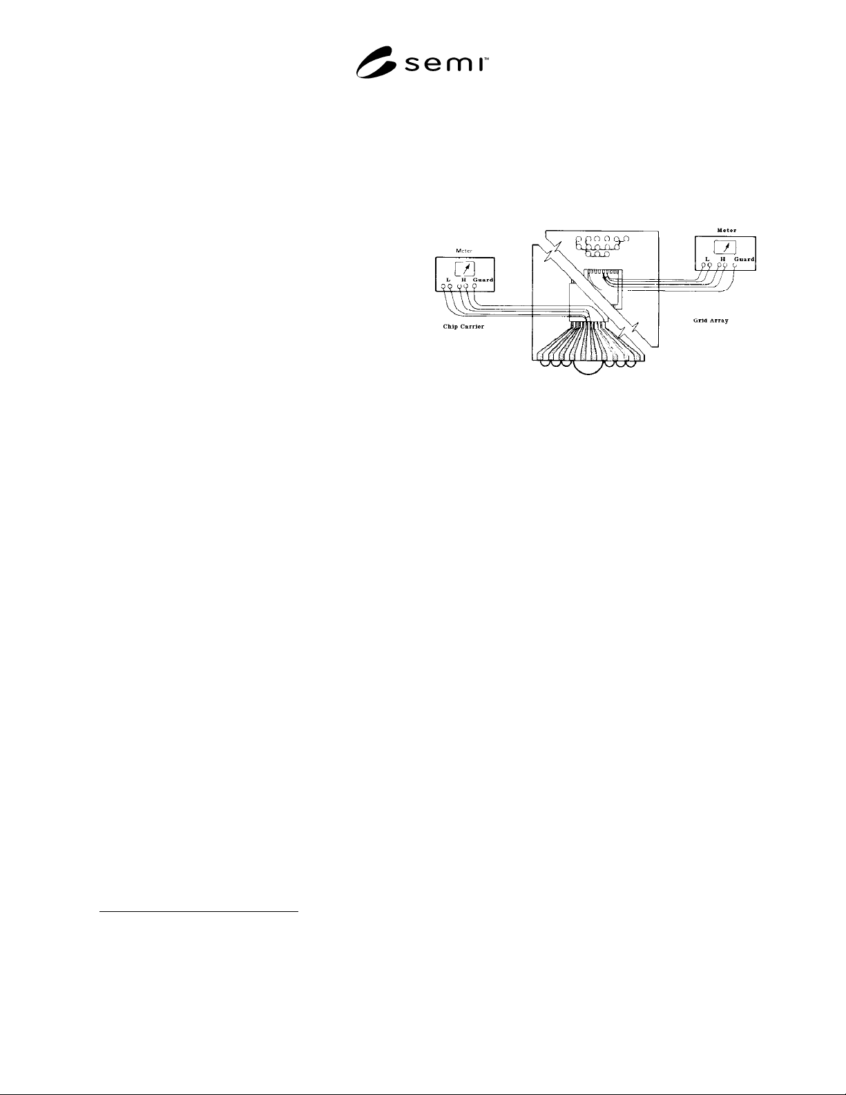
Figure 1
Lead-to-Lead Capacitance
3.2 Connect together all the pins in close proximity to
those being measured, for multi-layer ceramic package
pins should be chosen to connect all traces adjacent to
traces being measured. Example: Eight surrounding
pins are connected for the 68 lead pin grid; twelve
surrounding pins are connected together for the 124 pin
grid; eight surrounding pins are connected together for
all flat packs (see Figure 1). If there are power planes
and/or large power buses in the package, their pins must
be connected together with the eight or 12 surrounding
pins discussed above.
3.3 Place the guard probe down on the cavity side of
any one of the eight or 12 leads discussed in Section
3.2, to ensure that they will not affect the measurement.
3.4 Place one coaxial probe approximately 1/8 inch
above the cavity side of one of the leads to be
measured.
3.5 Place the other coaxial probe approximately 1/8
inch above the cavity side of the other lead to be
measured.
3.6 Nulling Procedure — If using an instrument that
auto-zeros, such as the H.P.4275A, follow the
instrument instructions for capacitance measurement. If
this type of instrument is not being used, take the
reading on the instrument at this point.
SEMI G24-89 © SEMI 1984, 1996 2
3.7 Place the probes down on the leads to be
measured. This should be a vertical movement only.
3.8 Take the capacitance reading. If using auto-
zeroing equipment, this capacitance measurement will
be used. If not, take the reading from 3.6 and subtract it
from the reading in 3.8 to derive the capacitance
measurement of interest. (See Table 1.)
Table 1 Capacitance Nulling Procedurefor Non-
Zeroing Equipment
Pins to be
Measured
Capacitance
Reading at
3.6
Capacitance
Reading at
3.8
Subtraction Step to
Derive Desired
Capacitance at 3.9
1 & 2 C
1
C
2
C
2
–C
1
= C
3
3 & 4 0.050 pf 2.130 pf 2.130–0.050 = 2.080
pf
For Auto-Zeroing Equipment:
Pins to be
Measured
Capacitance
Reading at
3.6
Capacitance
Reading at
3.8
Subtraction Step to
Derive Desired
Capacitance at 3.9
5 & 6 C
1
C
2
C
2
–C
1
= C
3
7 & 8 0.00 pf* 2.08 pf 2.080–0.000 = 2.080
pf
*Follow instrument instructions to read 0.00 pf
3.9 Repeat the procedure as required.
4 Procedure: Loading Capa citance
(See Figure 2)
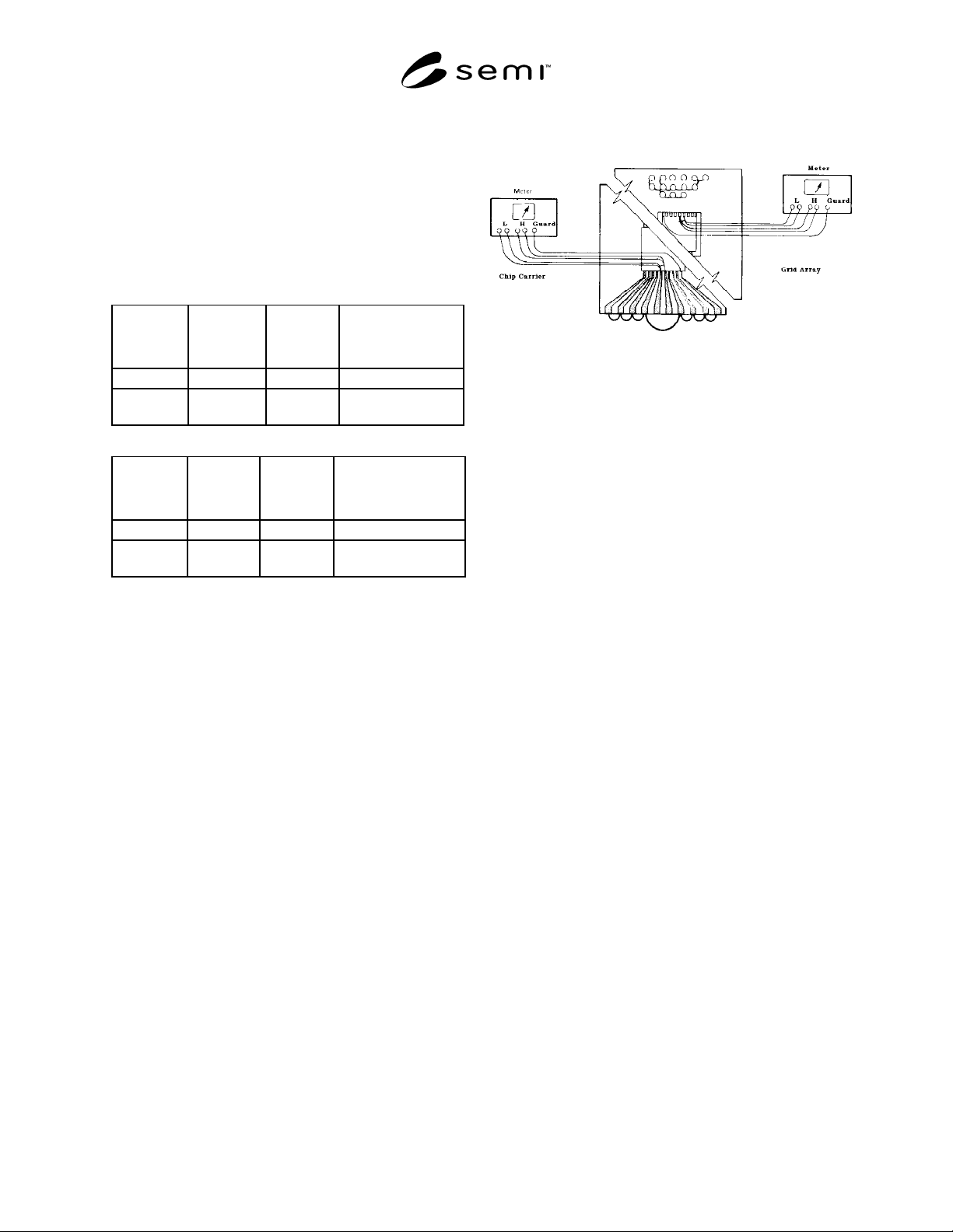
4.1 Omit guard terminal. Connect together all the pins
in close proximity to the one to be measured. Example:
Eight surrounding pins are connected together for the
68 pin grid; twelve surrounding pins are connected
together for the 124 pin grid; eight surrounding pins are
connected together for all flat packs (see Figure 2). If
there are power planes and/or large power buses in the
package, their pins must be connected together with the
eight or 12 surrounding pins discussed above.
4.2 Place one coaxial probe approximately 1/8 inch
above the cavity side of any one of the eight or 12 leads
discussed in Section 4.1.
Figure 2
Loading Capacitance
4.3 Place the other coaxial probe approximately 1/8
inch above the cavity side of the lead to be measured.
4.4 Continue as in Steps 3.6 to 3.9.
4.5 Overall accuracy with this method is ± 5%.
NOTICE: These standards do not purport to address
safety issues, if any, associated with their use. It is the
responsibility of the user of these standards to establish
appropriate safety and health practices and determine
the applicability of regulatory limitations prior to use.
SEMI makes no warranties or representations as to the
suitability of the standards set forth herein for any
particular application. The determination of the
suitability of the standard is solely the responsibility of
the user. Users are cautioned to refer to manufacturer’s
instructions, product labels, product data sheets, and
other relevant literature respecting any materials
mentioned herein. These standards are subject to
change without notice.
The user’s attention is called to the possibility that
compliance with this standard may require use of
copyrighted material or of an invention covered by
patent rights. By publication of this standard, SEMI
takes no position respecting the validity of any patent
rights or copyrights asserted in connection with any
item mentioned in this standard. Users of this standard
are expressly advised that determination of any such
patent rights or copyrights, and the risk of infringement
of such rights, are entirely their own responsibility.
Copyright by SEMI® (Semiconductor Equipment and Materials
International), 3081 Zanker Road, San Jose, CA 95134. Reproduction o
f
the contents in whole or in part is forbidden without express written
consent of SEMI.
SEMI G25-89 © SEMI 1984, 19891
SEMI G25-89
TEST METHOD FOR MEASURING THE RESISTANCE OF PACKAGE
LEADS
1 Purpose
This document defines the equipment, materials, and
procedure used to measure the resistance of leads in
packaging elements. This document uses a pin grid
(cavity down) package as one example of the type of
packaging element that can be measured with the
method described herein; however, this measurement
technique can be applied to other geometrics with
proper consideration.
2 Equipment and Materials
2.1 D.C. Ohmmeter which uses th e four point probe
(Kelvin) method with four cables. Minimum accuracy
should be ± 4 mΩ.
2.2 Probe station with four probes. Probes should be
such that the taper of the probe and the diameter of its
point allow two probes to come together within a 5 mil.
square without touching each other elsewhere.
Recommendation: Micromanipulator, four each, probe
number OON-FPC-6000 with #3 collet or equivalent.
3 Procedure
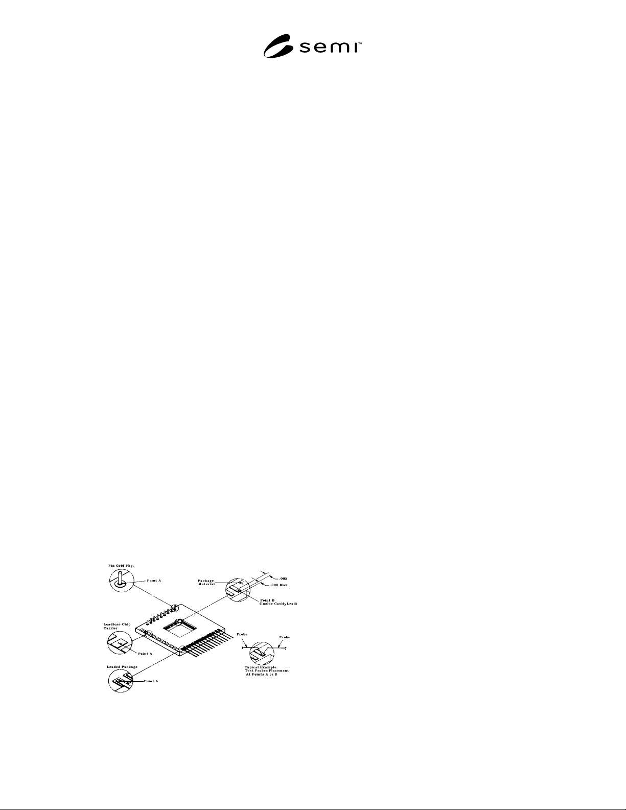
3.1 Place both probes of the low side of the meter as
close together as possible on the shoulder or in the
center of the outside lead (see Figure 1, Point A).
3.2 Place both probes of the high s ide of the meter
within 5 mils of the end of the lead on the cavity side of
the lead (see Figure 1, Point B).
3.3 Set the ohmmeter scale to the lowest setting
possible without putting meter in an “over range”
mode.
Figure 1
Resistance Measurement
3.4 Take resistance reading. Overall accuracy with this
method is ± 20 mΩ. This accuracy estimate includes
basic instrumentation error, probe placement
repeatability, and typical package construction (printed
pattern accuracy).=
4 Application Note
Readings below 100 mΩ can be made with acceptable
reeatability if considerable care in pleacement is taken.
For example, in measuring a conductor made of
tungsten 0.010" wide, a 0.010" variation in the distance
between the two sets of probes will result in a 15 mΩ
change in the measured reading. The same variation in
a gold conductor would result in a 3–5 mΩ error.
NOTICE: These standards do not purport to address
safety issues, if any, associated with their use. It is the
responsibility of the user of these standards to establish
appropriate safety and health practices and determine
the applicability of regulatory limitations prior to use.
SEMI makes no warranties or representations as to the
suitability of the standards set forth herein for any
particular application. The determination of the
suitability of the standard is solely the responsibility of
the user. Users are cautioned to refer to manufacturer’s
instructions, product labels, product data sheets, and
other relevant literature respecting any materials
mentioned herein. These standards are subject to
change without notice.
The user’s attention is called to the possibility that
compliance with this standard may require use of
copyrighted material or of an invention covered by
patent rights. By publication of this standard, SEMI
takes no position respecting the validity of any patent
rights or copyrights asserted in connection with any
item mentioned in this standard. Users of this standard
are expressly advised that determination of any such
patent rights or copyrights, and the risk of infringement
of such rights, are entirely their own responsibility.
Copyright by SEMI® (Semiconductor Equipment and Materials
International), 3081 Zanker Road, San Jose, CA 95134. Reproduction o
f
the contents in whole or in part is forbidden without express written
consent of SEMI.