semi合集-English.pdf - 第6324页
1 SEMI G64-96 © SEMI 1996, 2004 SEMI G64-96 (Reapproved 1104) SPECIFICATION FOR FULL-PLA TED INTEGRATED CIRCUIT LEADFRAMES (Au, Ag, Cu, Ni, Pd/Ni, Pd) This specification was technicall y reapproved by th e Global Assembl…
SEMI X##-#### © SEMI 2001 4
APPENDIX 1
NOTE: The material in this appendix is an official part of SEMI G63 and was approved by full letter ballot
procedures in 1995.
A1-1 Purpose
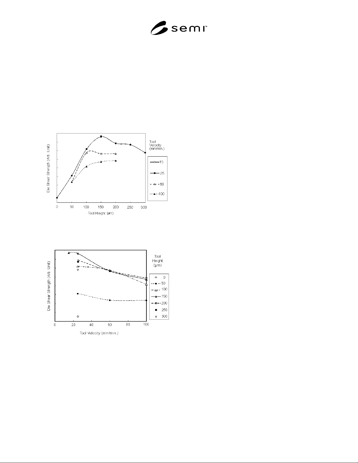
The purpose of this appendix is to indicate that speed
and height of the die contact tool affect die shear
strength results.
A1-2 Test Results
Figure A1-1
Tool Velocity Test Results
Figure A1-2
Tool Height Test Results
A1-2.1 Summary
A1-2.1.1 Shear Speed
a. Some adhesive might yield variable results due to
the relationship of the shear speed and failure
speed.
b. Some equipment with high shear speed could yield
low strength due to poor sensitivity at the peak of
the load.
A1-2.1.2 Height of the Die Contact Tool
a. In case of low height, fillet level might affect the
strength.
b. In case of high height, a variable result might be
obtained since the tool pulls the die and it tears the
adhesive.
NOTICE: SEMI makes no warranties or
representations as to the suitability of the standards set
forth herein for any particular application. The
determination of the suitability of the standard is solely
the responsibility of the user. Users are cautioned to
refer to manufacturer’s instructions, product labels,
product data sheets, and other relevant literature
respecting any materials mentioned herein. These
standards are subject to change without notice.
The user’s attention is called to the possibility that
compliance with this standard may require use of
copyrighted material or of an invention covered by
patent rights. By publication of this standard, SEMI
takes no position respecting the validity of any patent
rights or copyrights asserted in connection with any
item mentioned in this standard. Users of this standard
are expressly advised that determination of any such
patent rights or copyrights, and the risk of infringement
of such rights, are entirely their responsibility.
Copyright by SEMI® (Semiconductor Equipment and Materials
International), 3081 Zanker Road, San Jose, CA 95134. Reproduction o
f
the contents in whole or in part is forbidden without express writte
n
consent of SEMI.

1 SEMI G64-96 © SEMI 1996, 2004
SEMI G64-96 (Reapproved 1104)
SPECIFICATION FOR FULL-PLATED INTEGRATED CIRCUIT
LEADFRAMES (Au, Ag, Cu, Ni, Pd/Ni, Pd)
This specification was technically reapproved by the Global Assembly & Packaging Committee and is the
direct responsibility of the Japanese Packaging Committee. Current edition approved by the Japanese
Regional Standards Committee on July 23, 2004. Initially available at www.semi.org September 2004; to be
published November 2004. Originally published in 1996.
1 Purpose
1.1 This specification is intended as a guideline for
evaluating plating layer characteristics required by
users of full-plated leadframes for plastic
semiconductor packages.
1.2 Background — Full-plated leadframes have
received attention in recent years as a possible solution
to challenges and restrictions resulting from the effects
of Pb on the environment, package reliability
improvement due to the P.P.F. process, lead coplanarity
on fine-pitched leadframes, and lead bridges with solder
plating.
2 Scope
2.1 The specification and test procedures detailed in
this document apply to full-plated leadframes.
2.2 Units — SI units are used in this document.
NOTICE: This standard does not purport to address
safety issues, if any, associated with its use. It is the
responsibility of the users of this standard to establish
appropriate safety and health practices and determine
the applicability of regulatory or other limitations prior
to use.
3 Referenced Standards
3.1 SEMI Standards
SEMI G4 — Specification for Integrated Circuit
Leadframe Materials Used in the Production of
Stamped Leadframes
SEMI G18 — Specification Integrated Circuit
Leadframe Material Used in the Production of Etched
Leadframes
SEMI G21 — Specification for Plating Integrated
Circuit Leadframes
SEMI G52 — Standard Test Method for Measurement
of Ionic Contamination on Semiconductor Leadframes
(Proposed)
SEMI G55 — Test Method for Measurement of Silver
Plating Brightness
SEMI G56 — Test Method forMeasurement of Silver
Plating Thickness
3.2 ISO Standards
1
ISO-3497 — Metallic Coating Measurement of Coating
Thicknesses, X-Ray Spectrometer Method
ISO-9227 — Corrosion Tests in Artifical Atmospheres
- Salt Spray Tests
3.3 JIS Standard
2
JIS-C-0053 — Solderability Testing by the Wetting
Balance Method
3.4 Military and Federal Standards
3
MIL-C-14550 — Copper Plating-Electrodeposited
MIL-F-14256 — Flux, Soldering, Liquid, Paste Flux,
Solder Paste, and Solder Paste Flux
MIL-G-45204 — Gold Plating-Electrodeposited
MIL-STD-883D — Method 2003.7, Solderability
QQ-N-290 — Nickel Plating-Electrodeposited
QQ-S-365 — General Requirements for
Electrodeposited Silver Plating
QQ-S-571 — Solder Composition
NOTICE: Unless otherwise indicated, all documents
cited shall be the latest published versions.
4 Terminology
4.1 Definitions
4.1.1 finish plating — final plating layer whose
electrodeposits fulfill the main purpose of the required
characteristic.
1 International Organization for Standardization, ISO Central
Secretariat, 1, rue de Varembé, Case postale 56, CH-1211 Geneva 20,
Switzerland. Telephone: 41.22.749.01.11; Fax: 41.22.733.34.30,
Website: www.iso.ch
2 Japanese Industrial Standards, Available through the Japanese
Standards Association, 1-24, Akasaka 4-Chome, Minato-ku, Tokyo
107-8440, Japan. Telephone: 81.3.3583.8005; Fax: 81.3.3586.2014,
Website: www.jsa.or.jp
3 United States Military Standards, Available through the Naval
Publications and Forms Center, 5801 Tabor Avenue, Philadelphia,
PA 19120-5099, USA. Telephone: 215.697.3321
SEMI G64-96 © SEMI 1996, 2004 2
4.1.2 solderability — an index of the wettability and
coverage with solder of lead surface.
4.1.3 underplating — plating layers that complete the
required characteristics of the final plating layer and
lies between the base material and final plating layer.
5 Ordering Information
5.1 Priority
5.1.1 To avoid confusion, the order of precedence
when ordering leadframes shall be as follows:
1. Purchase Order (agreed between user and supplier)
2. This Specification
3. Referenced Documents
6 Materials
6.1 Base Material — Cu alloys or Fe/Ni alloys.
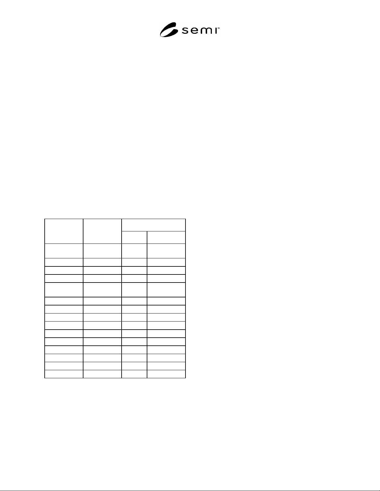
6.2 Plating Material — Underplating and Finish
plating are shown in Table 1.
Table 1 Table 1 Underplating and Finish Plating
Base Material
Finish Plating Underplating
Cu-Alloys Fe, Ni-Alloys
Au (MIL-G-
45204)
- N/A X
Ni X X
Ag (QQS-365) - X N/A
Cu X X
Cu (MIL-C-
14550)
- X X
Ni X X
Ni (QQN-290) - X X
Cu X X
Pd/Ni-Alloy - X X
Ni X X
Cu X X
Pd - X X
Ni X X
Cu X X
Pd/Ni-Alloy X X
7 Plating Specification
7.1 Plating Thickness — For full-plated leadframes, the
designed thickness including under plating is restricted
as follows to limit the effects of thickness variation on
coplanarity and outer lead width.
Designed thickness including under plating-1 / Ag-
plating: 5 µm MAX
Designed thickness including under plating-2 / Au,
Cu, Ni, Pd/Ni-Alloy, Pd plating: 2 µm MAX
7.2 Visual Inspection — Rejectable conditions are as
follows:
1. Any bare spots, or missing plating in critical area as
defined the coined areas or minimum flat wire bond
area in the appropriate leadframe specification.
2. Any peeling or blistered plating.
3. Any nodules in critical area as defined the coined
areas or minimum flat wire bond area in the
appropriate leadframe specification.
NOTE 1: Nodules not exceeding 0.0381 mm in a surface
dimension and 0.0127 mm in height, in non-critical areas
are allowed providing there are no more than one per
internal lead finger or six (6) per leadframe.
4. Any pits which exceed 0.008 mm in depth or 0.0127
mm in a surface dimension in critical areas or
0.0254 mm in depth or 0.051 mm in a surface
dimension in non-critical areas.
5. Any scratches or scrapes in the metallization plating
which expose underplating or base material.
6. Any scratches or scrapes in critical area which cause
a build up of material in excess of 0.0127 mm in
height.
7. Any foreign material, contamination, or tarnish.
8. Non-uniformity or rough-plated surface.
7.3 Visual Inspection after Baking — The test
procedure is described in Section 9.3. Visual inspection
after baking shall be performed according to the
procedure in Section 9.2.1.
7.4 Corrosion Resistance (not applicable to Cu
plating) — In the test result, allowable corrosion
specification shall be agreed upon between user and
supplier.
7.5 Surface Ion Contamination — Allowable ion
species and ion concentration shall be agreed upon
between user and supplier.
7.6 Adhesion — If there is any plating film on the test
tape, the component shall be rejected. Adhesive test
should be performed according to the procedure in
Section 9.6.
7.7 Functional Tests
7.7.1 Die Attach — Agreed upon between user and
supplier.