semi合集-English.pdf - 第972页
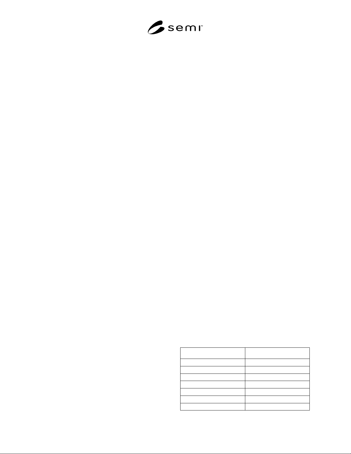
SEMI E129-1103 © SEMI 2003 10 Table A1-2 MM Classificatio n Levels Class Voltage, V M1 < 100 M2 100–199 M3 200–399 M4 ≥ 400 Table A1-3 CDM Classification Levels Class Voltage, V C1 < 125 C2 125–249 C3 250–499 C4 50…
SEMI E129-1103 © SEMI 2003 9
APPENDIX 1
DEVELOPING THE RECOMMENDATIONS FOR ELECTROSTATIC
LEVELS
NOTICE: This appendix offers information related to the Electrostatic Levels contained in Section 12.5. It was
approved as an official part of SEMI E129 by full letter ballot procedures on September 3, 2003.
A1-1 Recommended Levels
A1-1.1 The recommended charge and electrostatic
field levels in this guide are not based on specific
protection thresholds for individual devices or process
tools. Rather, their aim is to classify the types of ESD
events or static levels that are likely to be of concern.
Facility designers and users should determine the types
of events that are of most concern to their products and
processes, to apply this guide to their needs.
Information on specific device damage thresholds is
best determined on an individual basis.
A1-2 Justification of Guide Recommendations
in Section 12.5 Table 1
A1-2.1 Recommendations for ESD Damage
A1-2.1.1 An analysis of the recommended levels to
protect semiconductor devices is found in Appendix 1
of SEMI E78. Related Information 1 of SEMI E78
discusses test methods for determining ESD damage
thresholds for semiconductor devices. Devices are
qualified according to the highest ESD stresses they can
withstand without measurable change in their operating
parameters. This section attempts to develop guide
recommendations for minimizing ESD damage based
on those discussions in SEMI E78.
A1-2.1.2 The information contained in SEMI E78 was
developed with respect to semiconductors handled by
equipment. It was current when published in 1998.
Device damage thresholds continue to decrease as
geometries get smaller, and although the classification
systems discussed in SEMI E78 have not changed,
more devices are falling into the more sensitive
classifications.
A1-2.1.3 It is desirable in this document to avoid
confusion with SEMI E78 sensitivity levels, as well as
to synchronize with the major changes in technology
mapped in the International Technology Roadmap for
Semiconductors (ITRS). Recommendations for
acceptable static charge levels are listed in Section 12.5
Table 1 and given for the major technology nodes of the
2003 ITRS, which relate to the size of the features on
the wafer.
A1-2.2 Charge Levels for ESD Damage
A1-2.2.1 Related Information 1.1 discusses test
methods for determining ESD damage thresholds for
semiconductor devices. Devices are qualified
according to the highest ESD stresses they can
withstand without measurable change in their operating
parameters. This section attempts to develop guide
recommendations for minimizing ESD damage based
on the discussion in Related Information 1.1.
A1-2.2.2 As discussed in Related Information 1.1.3,
ESD Simulator testing uses different capacitances for
each model. For Human Body Model (HBM) it is 100
pF, for Machine Model (MM) it is 200 pF, and for
Charged Device Model (CDM) it depends on the
capacitance of the actual device being tested. In any
case, it is charge (charge = voltage × capacitance) that
damages the device. It would seem appropriate,
therefore, that the guide recommendations in Table 1 in
Section 12.5 be stated in units of charge (e.g., nC).
A1-2.2.3 Based on industry testing reflected in device
data sheets, there appears to be a wide range for ESD
immunity in semiconductor devices, and it depends on
the type of ESD simulator used. HBM-type ESD
discharges are due to personnel handling and not likely
to occur within equipment. Charged equipment parts
contacting devices (i.e., MM) and charged devices
contacting machine parts (i.e., CDM) are the most
likely causes of ESD damage to devices in equipment.
A1-2.3 Industry Device Damage Levels
A1-2.3.1 The recommended electrostatic levels are
based on the following industry classifications. Each of
the test methods, (i.e., HBM, MM, and CDM) have a
set of qualification levels defined. These are contained
in Tables A1-1, A1-2, and A1-3 below.
Table A1-1 HBM Classification Levels
Class Voltage, V
0 < 250
1A 250–499
1B 500–999
1C 1000–1999
2 2000–3999
3A 4000–7999
3B ≥ 8000
SEMI E129-1103 © SEMI 2003 10
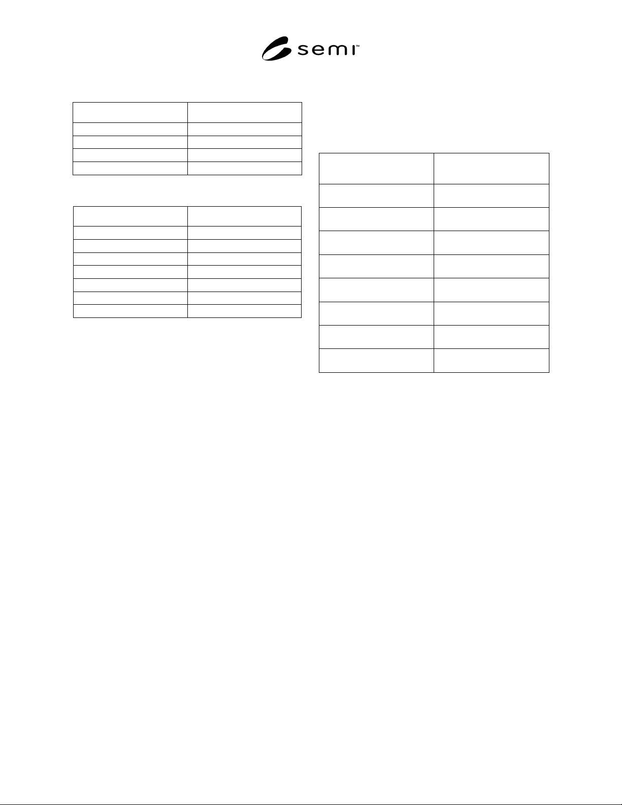
Table A1-2 MM Classification Levels
Class Voltage, V
M1 < 100
M2 100–199
M3 200–399
M4 ≥ 400
Table A1-3 CDM Classification Levels
Class Voltage, V
C1 < 125
C2 125–249
C3 250–499
C4 500–999
C5 1000–1499
C6 1500–1999
C7 ≥ 2000
A1-2.4 Guide Recommendations
A1-2.4.1 At the 180-nm technology node for the year
2000, it is assumed that devices (although some may
withstand higher levels of ESD) pass testing at HBM
Class 0 (250 V × 100 pF = 25 nC), MM Class M1 (100
V × 200 pF = 20 nC), and CDM Class C3 (500 V × 10
pF device capacitance = 5.0 nC).
A1-2.4.2 This guide recommends (Table 1 in Section
12.5) 2.5–10 nC at the 180-nm node in the year 2000. It
is assumed, for this and all further recommendations,
that the device capacitance is 10 pF.
A1-2.4.3 For major technology nodes, the allowable
ESD levels have decreased approximately with the
square of the ratio of the critical dimension. The
assumption is that energy dissipation capability is
proportional to the area of the feature.
A1-2.4.4 For example, in Table A1-4 at the 90-nm
node this guide recommends approximately 25% of the
180-nm node or 1 nC, at the 50-nm node the value has
changed to 0.25 nC, and at the 25-nm node the value is
0.1 nC. Intermediate technology years have been
changed accordingly.
A1-2.5 Recommendations for Particle Deposition
A1-2.5.1 SEMI E78 Related Information 1.2.2
discusses the enhancement of particle deposition due to
electrostatic fields from charges on the wafer surface.
This section attempts to develop the guide
recommendations for minimizing particle deposition
based on that discussion.
N/A = cv
elect
t (1)
where N/A equals the particle burden added to a wafer
during exposure time t, to a particle concentration c, in
an environment characterized by an electrostatic
particle deposition velocity, v
elect
.
Table A1-4 Guide Recommendations to Prevent ESD
Damage
Year
Node
Electrostatic Discharge,
nC
2000
180 nm
2.5–10
2002
130 nm
2.0
2003
100 nm
1.5
2004
90 nm
1.0
2007
65 nm
0.5
2009
50 nm
0.25
2012
32 nm
0.125
2015
25 nm
0.1
A1-2.5.2 Target values for N/A are given in the
International Technology Roadmap for Semiconductors
(ITRS 2002 Defect Reduction chapter). These target
values vary, depending on the type of product, the
critical dimensions of the technology, the type of
process, etc. An average of random particles added per
process step is developed, and for purposes of this
discussion will represent those resulting from particle
deposition. The variables c and t are process step
dependent and may or may not be controllable.
A1-2.5.3 The only variable in Equation 1 that depends
on electrical forces is v
elect
Both the particle charge and
the electric field in the vicinity of the wafer affect the
magnitude of v
elect
Particle charge is generally unknown
unless it is deliberately controlled by a neutralizing
action, and in the absence of this condition, a Fuchs-
type charge distribution is a reasonable assumption for
the particle charge. This assumption was used to
calculate the value of E
0
, the electric field at which v
elect
is equal to the particle deposition velocity from
diffusion (dominant for small particles).
A1-2.5.4 Using the process step values of c and t, and
the value of v
elect
calculated from Equation 10 in SEMI
E78 Related Information 1.2.2, the value of N/A for any
process step can be estimated. Alternatively, having
target values for N/A and c, and estimating the value of
v
elect
as outlined in the previous paragraph, allows one
to calculate the tolerable value of t:
SEMI E129-1103 © SEMI 2003 11
t = [N/A]/cv
elect
(2)
Using higher values of N/A in Equation 2 will increase
the acceptable values of t. Accepting higher values of c
will reduce max t.
A1-2.5.5 The value of the electrostatic field is initially
calculated at a distance of one wafer radius from the
wafer. While electrostatic field measurements can
certainly be made at this distance, they are typically
made at 2.5 cm (1 inch) with common instrumentation.
This is described in SEMI E43. Measurements made at
this smaller distance will be proportionally higher, but
under varying measurement conditions, it is difficult to
determine a precise relationship between electric field
and measurement distance. To provide a safety factor,
assume a linear relationship, rather than one
proportional to the square of the distance. For example,
with a 300-mm wafer, 3000 V/cm at 2.5 cm would
result in 500 V/cm at 15 cm.
A1-2.5.6 In SEMI E78, calculations were based on a
defect density N/A = 0.016 defects/cm
2
and a deposition
velocity v
elect
of 0.0105 cm/s. An example of the
resulting calculations is found in SEMI E78 Appendix 1
Table A1-2.2, a portion of which is shown in Table A1-
5.
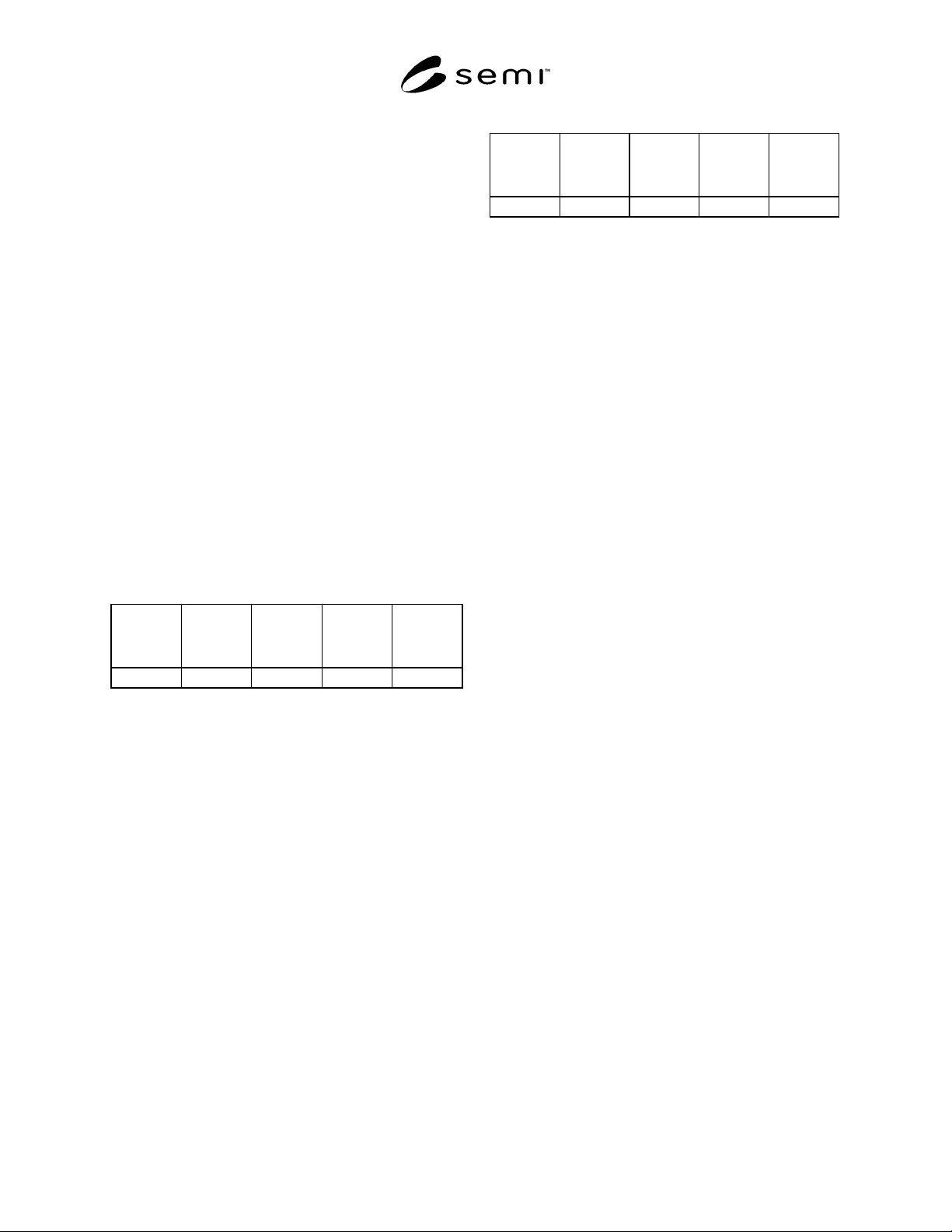
Table A1-5 SEMI E78 Guide Table A1 – 2.2
E,
V/cm at
2.5 cm
N/A,
defects/
cm
2
v
elect
,
cm/s
ct,
s/cm
3
max t in
Class 1,
s
200 0.016 0.0105 1.524 1220
A1-2.5.7 Tables A1-6 and A1-7 below are derived
from Table A1-5 above, which is taken from SEMI E78
Appendix A1-2.2.2. They contain the same
assumptions used for the SEMI E78 table, but reflect
values for defect density (N/A) and particle deposition
velocity contained in the ITRS 2002 document for each
technology node. Assumptions are:
• Calculations are made for ISO Class 3 (formerly
Federal Standard 209E Class 1) where c ≤ 0.00124
particles/cm
3
.
• As contained in both the 1999 and 2002 ITRS,
particle deposition velocity is assumed to be 0.01
cm/s (2002 ITRS Yield Enhancement Chapter,
Notes Table 95a). Calculations are made assuming
the electrostatic deposition velocity, v
elect
, is equal
to this value.
• For N/A = 0.0141 defects/cm
2
as specified in the
1999 ITRS for the 180-nm node (Defect Reduction
Chapter, Table 77, assuming “Random Defects”
per mask layer are all the result of particle
deposition), the corresponding table becomes:
Table A1-6 Modified SEMI E78 Guide Table A1 – 2.2
E,
V/cm at
2.5 cm
N/A,
defects/
cm
2
v
elect
,
cm/s
ct,
s/cm
3
max t in
Class 1,
s
190 0.0141 0.01 1.41 1140
• The values from the 2002 ITRS (Yield
Enhancement Chapter, Table 91) N/A = 0.0093
defects/cm
2
as specified for the 130-nm node,
0.0089 defects/cm
2
for the 100-nm node, 0.0059
for the 65-nm node, 0.0056 for the 45-nm node,
0.0043 for the 32-nm node, and 0.0044 for the 22-
nm node technology are used.
• Calculations are normalized for an exposure time
of 1200 s (i.e., E values multiplied by 1140/1200).
• Relationship of electrostatic field, technology node,
and constant airborne particle concentration are
shown in Table A1-7.
• The years and technology nodes shown in Table
A1-7 correspond to those to be used in the 2003
ITRS.
A1-2.6 Recommendations for Induced ESD Damage
A1-2.6.1 The presence of electrostatic fields in
semiconductor manufacturing areas also creates the
potential for induced ESD damage. When an isolated
conductor is placed in an electric field, a charge
separation occurs in the conductor. If the conductor
momentarily touches ground, a flow of charge will
occur to the conductor. This flow of charge is a
potentially damaging ESD event. If the conductor, now
possessing excess charge, is removed from the electric
field, a second ESD event can occur when the
conductor contacts ground again.
A1-2.6.2 The most obvious example of these
phenomena occurs once the semiconductor device is
packaged. The package material is epoxy, an easily
charged insulator. The electric field from the charged
package induces a charge on the device leads. ESD
events occur when the leads contact ground during
processing.