semi合集-English.pdf - 第5862页
SEMI P34-0200 © SEMI 2000 5 Table 4 Fused Sil ica Substrate Defect Limits Bulk Defects With in the Visual Q uality Area Opaque Spots Bubble Total Defec ts (per cm 2 )N o t e s > 1 µ m> 1 µ m 01 , 2 ≤ 1 µ m ≤ 1 µ m …
SEMI P34-0200 © SEMI 2000 4
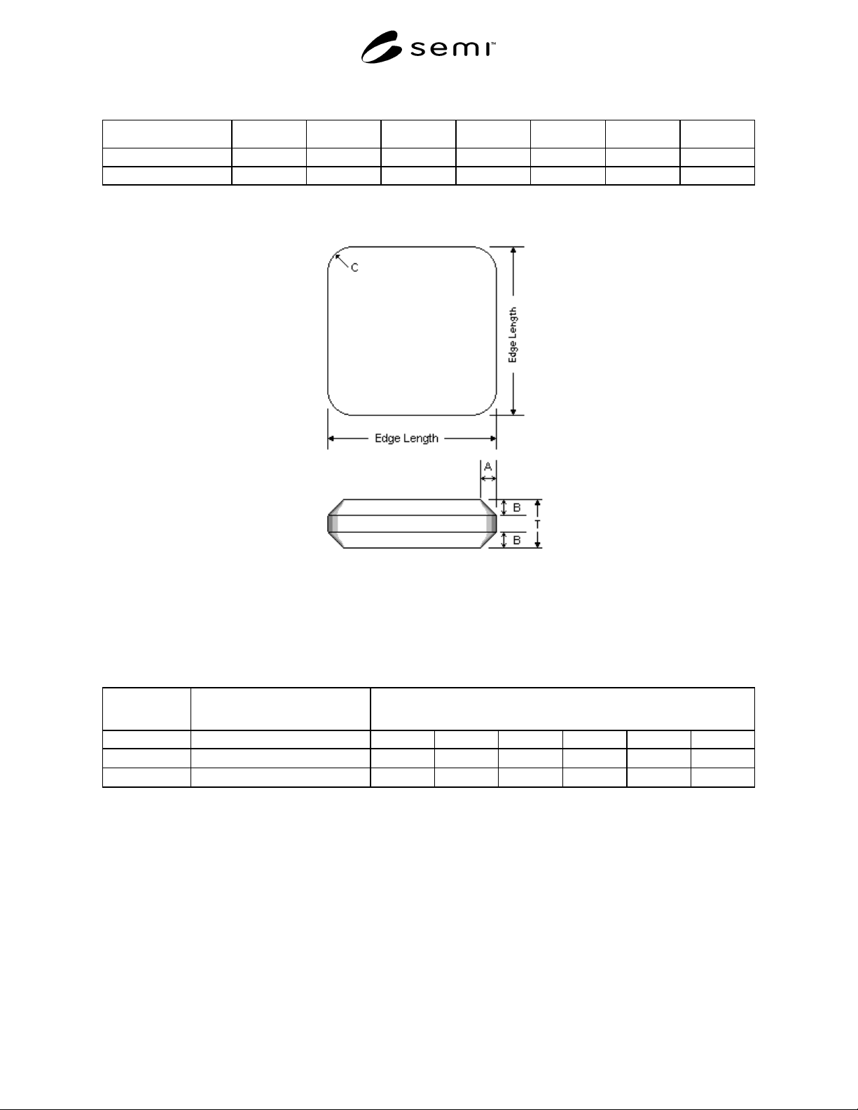
Table 2 Specifications for Chamfered Edge Dimensions
TAABBCC
Nominal Min. Max. Min. Max. Min. Max. Units
9.00 0.20 0.60 0.20 0.60 2.00 3.00 mm
Figure 3
Dimensions for Chamfered Edge and Rounded Corners
Note: “C” is radius of curvature of corners.
Table 3 Substrate Material Characteristics
Fused Silica Coefficient of Expansion (°C
–1
)
between 0°C and 300°C
Minimum Transmittance (%) of 9 mm Thick Substrate at Wavelengths of:
193 nm 248 nm 254 nm 365 nm 405 nm 436 nm
Virgin
< 7.5 × 10
–7
90 90 90 90 90 90
Repolished
< 7.5 × 10
–7
89 90 90 90 90 90
SEMI P34-0200 © SEMI 20005
Table 4 Fused Silica Substrate Defect Limits
Bulk Defects Within the Visual Quality Area
Opaque Spots Bubble Total Defects (per cm
2
)Notes
> 1 µm> 1 µm
01, 2
≤ 1 µm ≤ 1 µm
0.0078
Surface Defects Within the Visual Quality Area
Residue Scratch Size Total Scratch
Defects
Sleek Size Total Sleek Defects
(per cm
2
)
Opaque Spot
Size
Total Opaque Spot
Defects (per cm
2
)
Critical side None
> 1.0 µm
0
> 1.0 µm
0
> 1.0 µm
0
≤ 1.0 µm
no limit
≤ 1.0 µm
0.0465
≤ 1.0 µm
0.0155
Non-critical side
> 1.0 µm
0
> 3.0 µm
0.0465
≤ 1.0 µm
no limit
≤ 3.0 µm
no limit
Defects Outside the Visual Quality Area
Defect Limit Total Number Notes
Edge Chips Radial Depth
≥ 0.76 mm
03
Peripheral Chord
≥ 0.76 mm
03
Other Shall be negotiated between user and
supplier.
Shall be negotiated between user and
supplier.
NOTES:
1. The size of internal defects is defined as 1/2 (long axis + short axis).
2. This table is based on the assumption that defects < 1 µm will fall outside the focal depth of the lens systems and should not print.
3. None of any size permitted that break the surface.
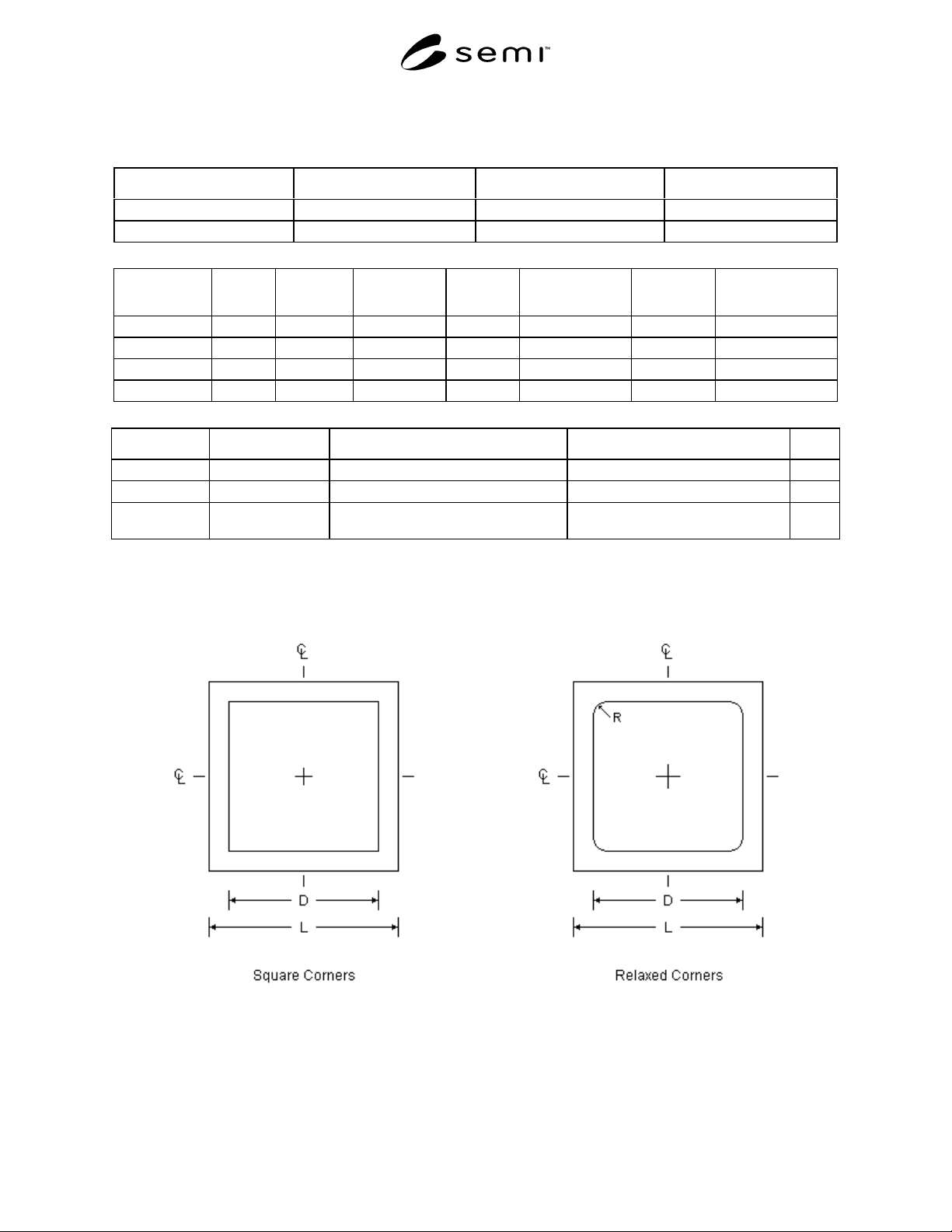
D ≥ 213 mm
R ≤ 6.5 mm (radius of curvature)
Figure 4a Figure 4b
Square Flatness Quality Area Relaxed Square Flatness Quality Area
SEMI P34-0200 © SEMI 2000 6
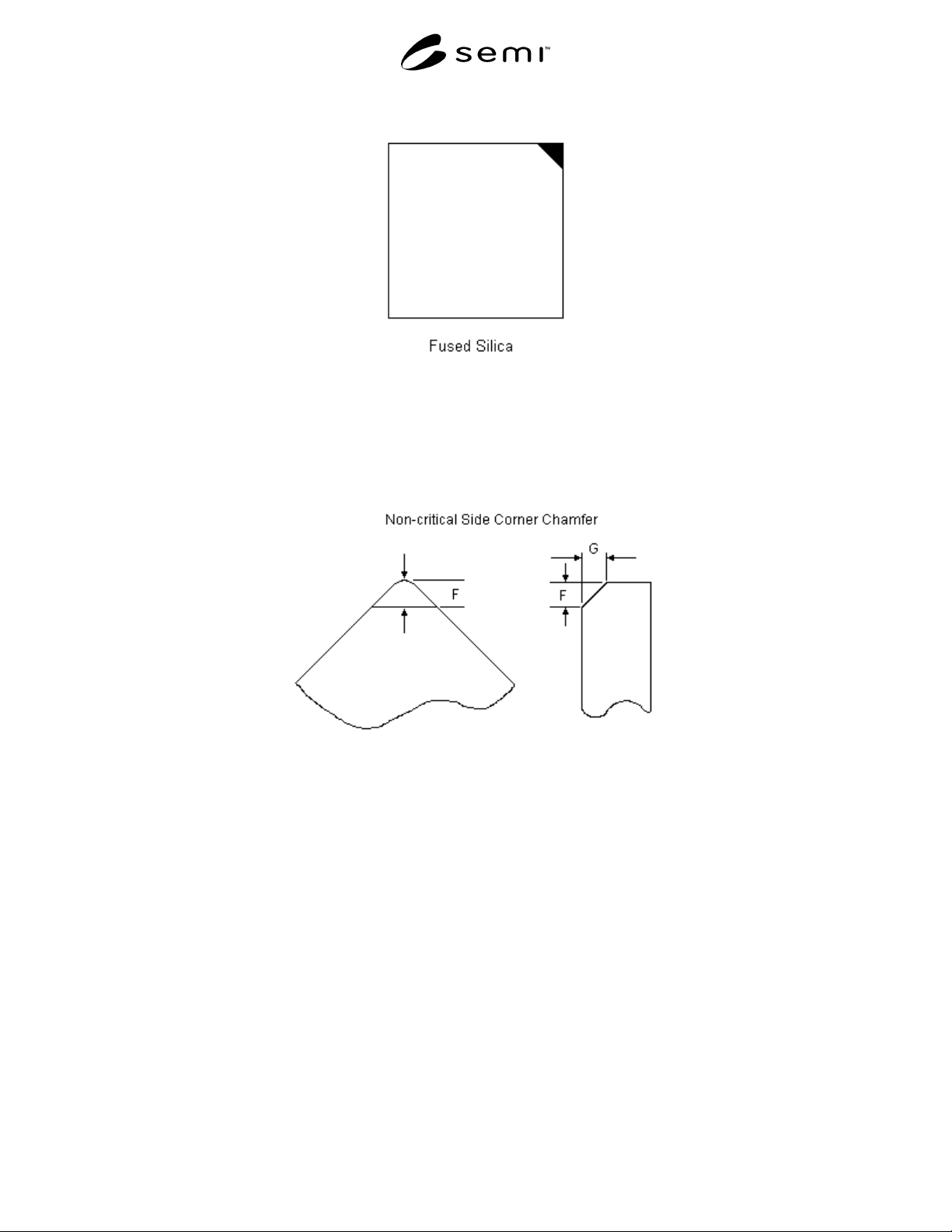
Figure 5
Substrate Identification by Corner Chamfer
(Non-critical Side)
F = 1.5–2.0 mm
G = 0.6–1.0 mm
Figure 6
Dimension of Corner Chamfer
(Edge Chamfer Not Indicated)