semi合集-English.pdf - 第6406页
SEMI G74-0699 © SE MI 1998, 1999 3 6.2 Sur face Hardness — HRc ≥ 47 6.3 Resiliency — Must return to o r i gi nal shape, where the linear s cale ruler reads 0, af ter one side is held f ir m and t he ot her is bent wi th …
SEMI G74-0699 © SEMI 1998, 1999 2
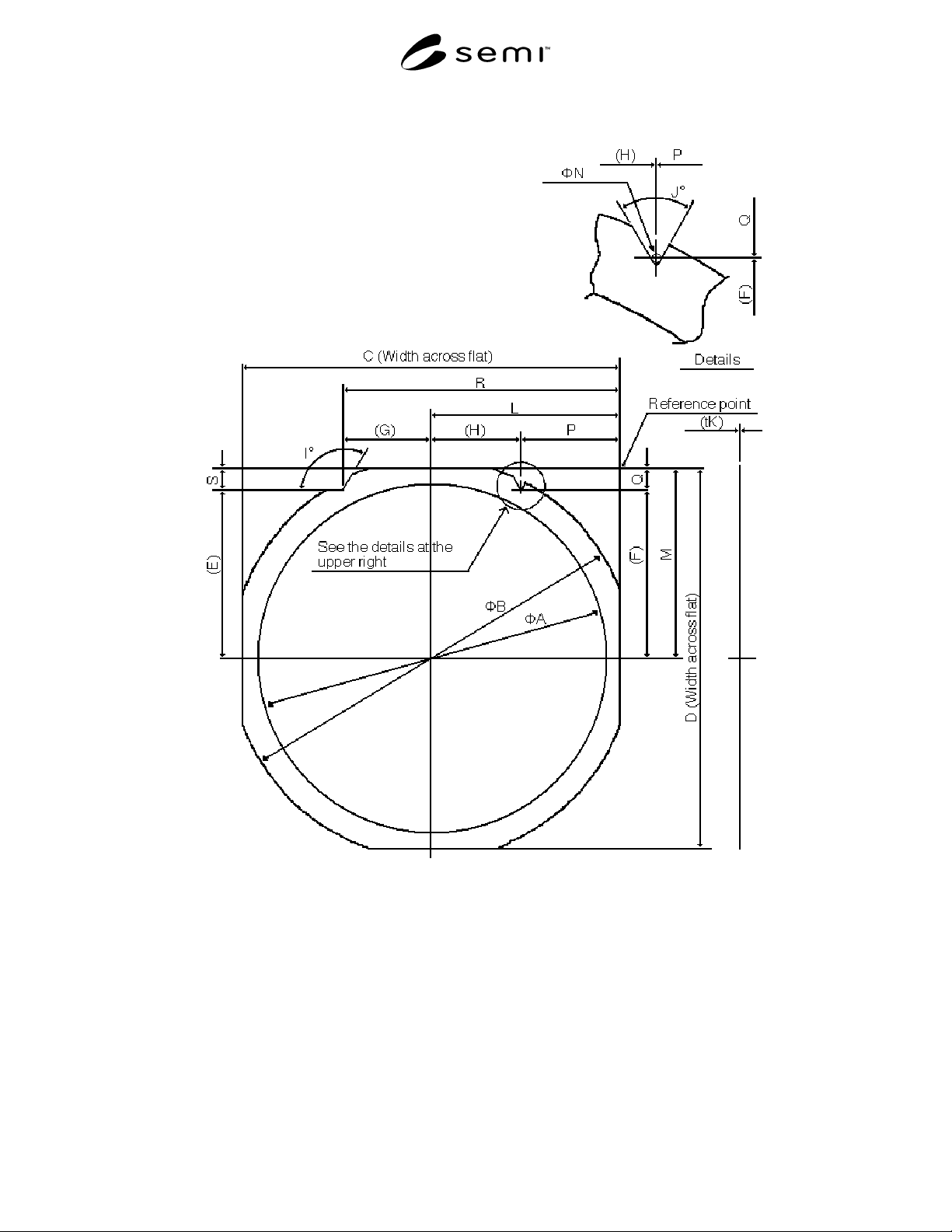
Figure 1
300 mm Tape Frame Dimensions

SEMI G74-0699 © SEMI 1998, 19993
6.2 Surface Hardness — HRc ≥ 47
6.3 Resiliency — Must return to original shape, where
the linear scale ruler reads 0, after one side is held firm
and the other is bent with a force of 30 N for 60
seconds.
6.4 Surface Roughness — R
a
≤ 0.1 µm, R
max
is within
≤ 1.0 µm
6.5 Flatness — Within 0.3 mm
7 Test Methods
7.1 Dimensions — To be measured with a measuring
device, such as a caliper, with a precision of 0.05 mm.
7.2 Surface Hardness — To be me asured according to
the method in JIS Z2245 with a Rockwell Hardness
Tester.
7.3 Resiliency — Secure one side of the frame in a
vice, and bend with a force of 30 N for 60 seconds.
After that, release the frame and measure the change
from the original shape with a linear scale ruler. The
linear scale ruler should have a precision of at least 0.5
mm.
7.4 Surface Roughness — Measur e with a surface
roughness gauge. Surface roughness is measured
perpendicular to the undulation and must be shown as
roughness average (R
a
) and maximum peak-to-valley
roughness height (R
max
). Refer to ISO4287 Part 1, JIS
B0601, and ANSI/ASME B46.1.
7.5 Flatness — Place the frame on a surface with
near-zero flatness. Measure the lowest point and the
highest point on the frame with a height gauge, and
record the difference in these values. Turn the frame
over and repeat the process. The flatness will be the
larger of the two values.
8 Certification
8.1 Upon request of the purchaser in the contract or
order, a manufacturer's or supplier's certification that
the material was manufactured and tested in accordance
with this specification, together with a report of the test
results, shall be furnished at the time of shipment.
9 Packing and Package Lab eling
9.1 The product must be packaged appropriately to
prevent deformities, moisture, and contamination, as
well as damage during normal shipping.
9.2 The products must be clearly m arked with the
purchase number, quantity, gross weight, and supplier's
name.
9.3 Special packaging and delivery requests will be
decided between the supplier and the purchaser at time
of purchase.
9.4 Surface Hardness — HRc ≥ 47
9.5 Resiliency — Must return to o riginal shape, where
the linear scale ruler reads 0, after one side is held firm
and the other is bent with a force of 30 N for 60
seconds.
9.6 Flatness — Within 0.3 mm
SEMI G74-0699 © SEMI 1998, 1999 4
APPENDIX 1
BARCODE LABEL POSITIONS FOR 300 MM TAPE FRAMES
NOTE: The material in this appendix is an official part of
SEMI G74 and was approved by full letter ballot procedures
on March 17, 1999.
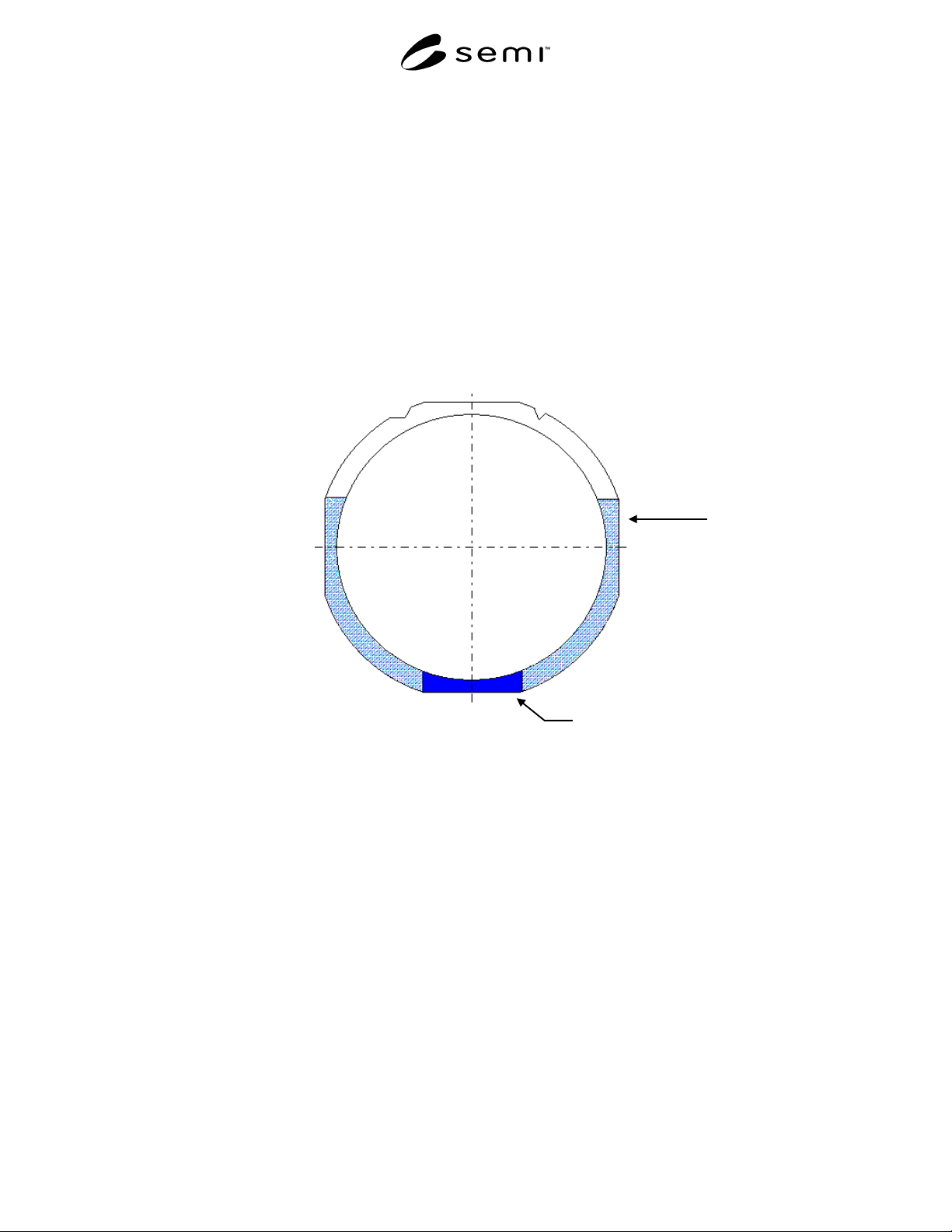
A-1 Barcode Label Positions
A-1.1 The recommended position for the barcode label
is position (A in Figure A1-1).
A-1.2 However, it is acceptable if the barcode labels
are within the shaded area (see B in Figure A1-1).
A-2 Reasons to recommend position (A)
A-2.1 It is easier to detect whether there are any
barcode labels or not, without pulling out the frames.
A-2.2 It is convenient to have the labels on the
opposite side of the notches, as the frames are normally
pulled out from the notch side.
Figure A1-1
Barcode Label Positions
NOTICE: These standards do not purport to address
safety issues, if any, associated with their use. It is the
responsibility of the user of these standards to establish
appropriate safety and health practices and determine
the applicability of regulatory limitations prior to use.
SEMI makes no warranties or representations as to the
suitability of the standards set forth herein for any
particular application. The determination of the
suitability of the standard is solely the responsibility of
the user. Users are cautioned to refer to manufacturer's
instructions, product labels, product data sheets, and
other relevant literature respecting any materials
mentioned herein. These standards are subject to
change without notice.
The user's attention is called to the possibility that
compliance with this standard may require use of
copyrighted material or of an invention covered by
patent rights. By publication of this standard, SEMI
takes no position respecting the validity of any patent
rights or copyrights asserted in connection with any
item mentioned in this standard. Users of this standard
are expressly advised that determination of any such
patent rights or copyrights, and the risk of infringement
of such rights, are entirely their own responsibility.
A
B
Copyright by SEMI® (Semiconductor Equipment and Materials
International), 3081 Zanker Road, San Jose, CA 95134. Reproduction o
f
the contents in whole or in part is forbidden without express written
consent of SEMI.