semi合集-English.pdf - 第6511页
SEMI G80-0200 © SE MI 2000 19 Table 2 (cont .) Test Method S ummar y - Non Data Analy sis Aspects Associate d with This Method 1. Level 1 –– Procedu r e Start Dat e and Time: 4. L evel 2 –– Procedure F inis h Data and Ti…
SEMI G80-0200 © SEMI 2000 18
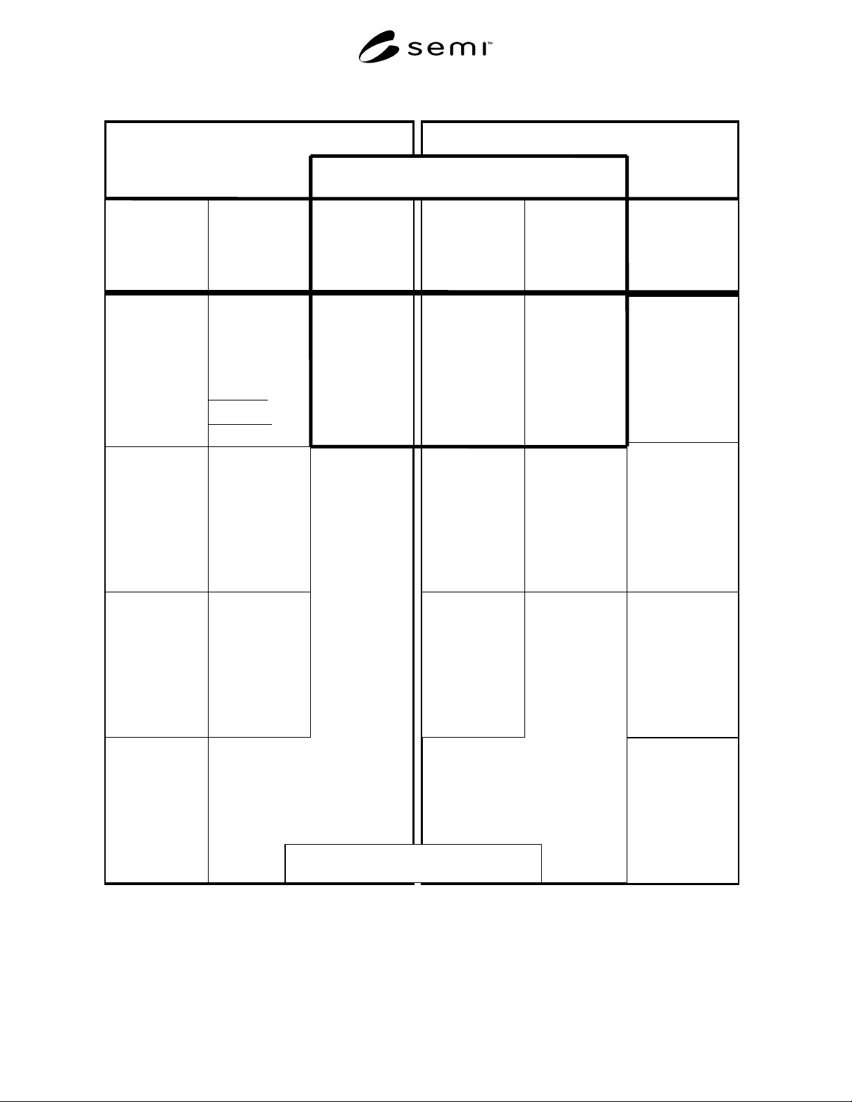
Table 2 Test Method Summary Table for Establishing Overall Timing Accuracy (OTA)
LEVEL 1
Timing Linearity
Extended Delay
Multiple Period
Data below represents
Level 1edge-delay results
LEVEL 2
High Speed Clock
Accuracy
Data to enter here =
"a" below:
Drive Input Z
Timing Error Level
1 (Section 10.3.5) Z
to 0 (Low)-
Data to enter here is
Positive Error and
Negative Error per
the data in Table 1
and Equation 1
Appendix 2.
Timing Linearity
Level 1 (Sec.10.3.1)
Data to enter here is
Positive Error &
Negative Error per
the data in Table 1
and the 2 equations:
Positive Error =
Reference - Max Value
N
egative Error =
Reference -Min Value
d) High Speed Clock
Self Trigger Phase
Jitter Level 2 (Section
10.4.6)-
Data to enter here =
the RMS value in
Table 1.
c) High Speed Clock
Self Trigger
Cycle Jitter Level 2
(Section 10.4.5)
Data to enter here =
the RMS value in
Table 1.
Extended Delay
Level 1 (Sec.
10.3.4)- Data to
enter here is
Positive Error and
Negative Error per
the data in Table 1
and Equation 1
Appendix 2.
Multiple Period
Level 1 Optional
(Sec. 10.3.6) Data
to enter here is
Positive Error and
Negative Error per
the data in Table 1
and Equation 1
Appendix 2.
Drive Input Z
Timing Error Level
1 (Section 10.3.5) Z
to 1 (High)-
Data to enter here is
Positive Error and
Negative Error per
the data in Table 1
and Equation 1
Appendix 2.
Drive Input Z
Timing Error Level
1 (Section 10.3.5) 0
(Low) to Z -
Data to enter here is
Positive Error and
Negative Error per
the data in Table 1
and Equation 1
Appendix 2.
Drive Input Z
Timing Error Level
1 (Section 10.3.5) 1
(High) to Z-
Data to enter here is
Positive Error and
Negative Error per
the data in Table 1
and Equation 1
Appendix 2.
1) Drive Input To
Compare Output
Timing
Data to enter here is
Drive Input to Compare
Output (value below)
3) Compare Output
Edge Placement
Data to enter here = a)
Compare Output Time
Delay Error
2) Drive
Input Edge
Placement
Data to enter here =
"a" below:
Drive Input to
Compare Out put
Timing Accuracy
calculated from
10.3.1 data as:
Reference -
[(MinValue+Max
Value)/2]. Refer to
examples in
Appendix 2.
a) Compare Output
Time Delay Error
Level 2 (Section
10.4.2) Data to
enter here = the
delta between the
min and max values
in Table 1.
a) Drive Input
Timing Delay Error
Level 2 (Section
10.4.1)-
Data to enter here =
the delta between
the min and max
values in Table 1.
b) Drive Input
Transition Time
Variation
Level 2 (Section
10.4.3) -
Data to enter here =
the delta between
the min and max
values in Table 1.
b) Compare Output
Timing Jitter
(Note: no method
exists for this test)
c) Drive Input
Timing Cycle Jitter
Level 2 (Section
10.4.4)
Data to enter here =
the RMS value in
Table 1.
Single Point Overall Timing Accuracy (OTA) Results
Data to enter here is: A = Dr (item 2) + Cmp (item 3) + Dr-Cmp (item 1)
-B = -Dr (item 2) - Cmp (item 3) + Dr-Cmp (item 1)
.
Drive Z Timing
Data below represents
Level 1 Z- state timing
results
a) High Speed Clock
Delay Error (Section
10.4.1- same as Drive
Input Timing Delay
but for clock pins)
Data taken and
entered for these pins
equivalent to Drive
Input Timing
b) High Speed Clock
Transition time
variation (Section
10.4.3- same as drive
input transition time
but for clock pins)
Data entry equivalent
to Drive Input
Transition Time.
The user of the method is advised to read Section
13, Precautions before filling in this table.
SEMI G80-0200 © SEMI 200019
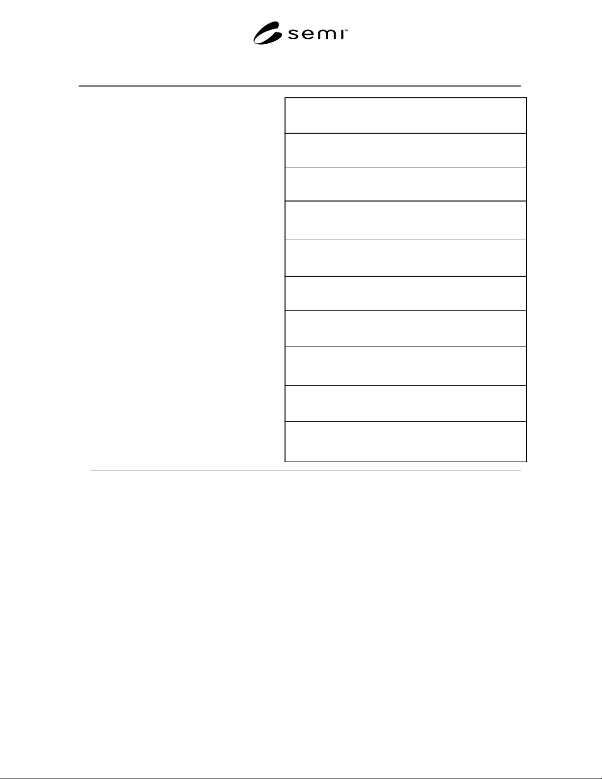
Table 2 (cont.) Test Method Summary - Non Data Analysis Aspects Associated with This Method
1. Level 1 –– Procedure Start Date and Time:
4. Level 2 –– Procedure Finish Data and Time:
5. Specify the Ambient Temperature when this
method was executed.
6. Manufacturer's model number and/or name for
this system analyzed.
7. System Serial Number:
8. Date & Time of Last System Calibration:
9. Specify PARTIAL or Full-Up execution of
this method. Exceptions noted in Appendix 3.
3. Level 2 –– Procedure Start Date and Time:
2. Level 1 –– Procedure Finish Date and Time:
10. Specify Number of Test Heads & Number of
Pins analyzed using this method.
SEMI G80-0200 © SEMI 2000 20
APPENDIX 1
NOTE: The material in this appendix is an official part of SEMI G80 and was approved by fulll letter ballot procedures on
September 3, 1999 by the North Amerian Regional Standards Committee.
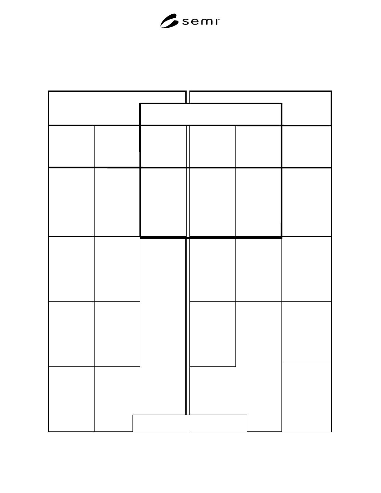
Table A1-1 Test Method Summary Table for Establishing Overall Timing Accuracy (OTA)
LEVEL 1
Timing Linearity
Extended Delay
Multiple Period
Data below represents
Level 1 edge-delay
results
LEVEL 2
High Speed Clock
Accuracy
_
_________________
_
Drive Input Z
Timing Error
Level 1 (Section
10.3.5) Z to 0
(Low)
_
_____________
_
_____________
Timing Linearity
Level 1
(Sec.10.3.1)
Positive Error:
_________________
Negative Error:
_________________
b) High Speed
Clock Transition
Time Variation
Level 2 (Section
10.4.3- Drive Input
Transition Time
for clock function)
_
______________
a) High Speed
Clock Delay Error
Level 2 (Section
10.4.1- Drive Input
Timing Delay for
clock function)
_
______________
Extended Delay
Level 1 (Sec.
10.3.4)
Positive Error:
_________________
Negative Error:
_
_______________
Multiple Period
Level 1 Optional
(Sec. 10.3.6)
Positive Error:
_________________
Negative Error:
_
________________
Drive Input Z
Timing Error
Level 1 (Section
10.3.5) Z to 1
(High)
_
_____________
_
_____________
Drive Input Z
Timing Error
Level 1 (Section
10.3.5) 0 (Low)
to Z
_
_____________
_
_____________
Drive Input Z
Timing Error
Level 1 (Section
10.3.5) 1 (High)
to Z
_
_____________
_
_____________
1) Drive Input
To Compare
Output Timing
_
_______________
_
3) Compare
Output Edge
Placement
_
_______________
2) Drive
Input Edge
Placement
_
_______________
_
Drive Input to
Compare Out put
Timing Accuracy
calculated from
the 10.3.1 entry.
_
_____________
a) Compare
Output Time
Delay Error
Level 2 (Section
10.4.2)
_
_____________
a) Drive Input
Timing Delay
Error Level 2
(Section 10.4.1)
_
_____________
b) Drive Input
Transition Time
Variation
Level 2 (Section
10.4.3)
_
_____________
c) Drive Input
Timing Cycle
Jitter Level 2
(Section 10.4.4)
_
____________
Single Point Overall Timing Accuracy (OTA) Results
D
ata to enter here is: A = Dr (item 2) + Cmp (item 3) + Dr-Cmp (item 1)
-B = -Dr (item 2) - Cmp (item 3) + Dr-Cmp (item 1)
.
Drive Z Timing
Data below
represents Level 1 Z-
state timing results
c) High Speed
Clock Cycle Jitter
Level 2 (Section
10.4.5)
_
______________
d) High Speed
Clock Phase Jitter
Level 2 (Section
10.4.6)
_
______________
The user of the method is advised to read Section
13, Precautions before filling in this table.