semi合集-English.pdf - 第5333页
SEMI M51-0303 © SEMI 2002, 2003 11 RELATED INFORMATION 1 OUTLINE OF ROUND ROBIN NOTICE: This related inf ormation is not an of ficial part of SEM I M51 and is not i n tende d to modify or s upersede the propose d standa …

SEMI M51-0303 © SEMI 2002, 2003 10
12.4.1 Histogram and Weibull plot of breakdown
electric field
12.4.2 Average of breakdown voltage, breakdown
electric field
12.4.3 Breakdown mode yield (A-mode, B-mode and
C-mode)
12.4.4 Breakdown mode map or E
bd
map
12.4.5 Result of calculated defect density
NOTICE: SEMI makes no warranties or
representations as to the suitability of the standards set
forth herein for any particular application. The
determination of the suitability of the standard is solely
the responsibility of the user. Users are cautioned to
refer to manufacturer's instructions, product labels,
product data sheets, and other relevant literature,
respecting any materials or equipment mentioned
herein. These standards are subject to change without
notice.
By publication of this standard, Semiconductor
Equipment and Materials International (SEMI) takes no
position respecting the validity of any patent rights or
copyrights asserted in connection with any items
mentioned in this standard. Users of this standard are
expressly advised that determination of any such patent
rights or copyrights, and the risk of infringement of
such rights are entirely their own responsibility.
SEMI M51-0303 © SEMI 2002, 2003 11
RELATED INFORMATION 1
OUTLINE OF ROUND ROBIN
NOTICE: This related information is not an official part of SEMI M51 and is not intended to modify or supersede
the proposed standard. It is provided for information purposes.
R1-1 MOS Structure
R1-1.1 Gate Oxide Thickness
R1-1.1.1 In this round robin, we evaluated the GOI of
MOS capacitors with a gate oxide film thickness of 25
nm on mirror-polished, p-type, CZ silicon wafers. In
the TZDB evaluation, a negative electric field was
applied step by step from 0 to 15 MV/cm, and an oxide
leakage current value was measured. When the oxide
leakage current first exceeded the dielectric breakdown
judgment value, we judged that the gate oxide film
dielectrically broke down.
0.01
0.10
1.00
10.00
100.00
0.01 0.10 1.00 10.00 100.00
Defect Density by OPP [cm
-2
]
Defect Density by TZDB [cm
-2
]
C
G
OPP Defect Density (cm
-2
) =
OPP-data x 10
-5
cm
T
ox
= 25 nm
S
=
10 mm
2
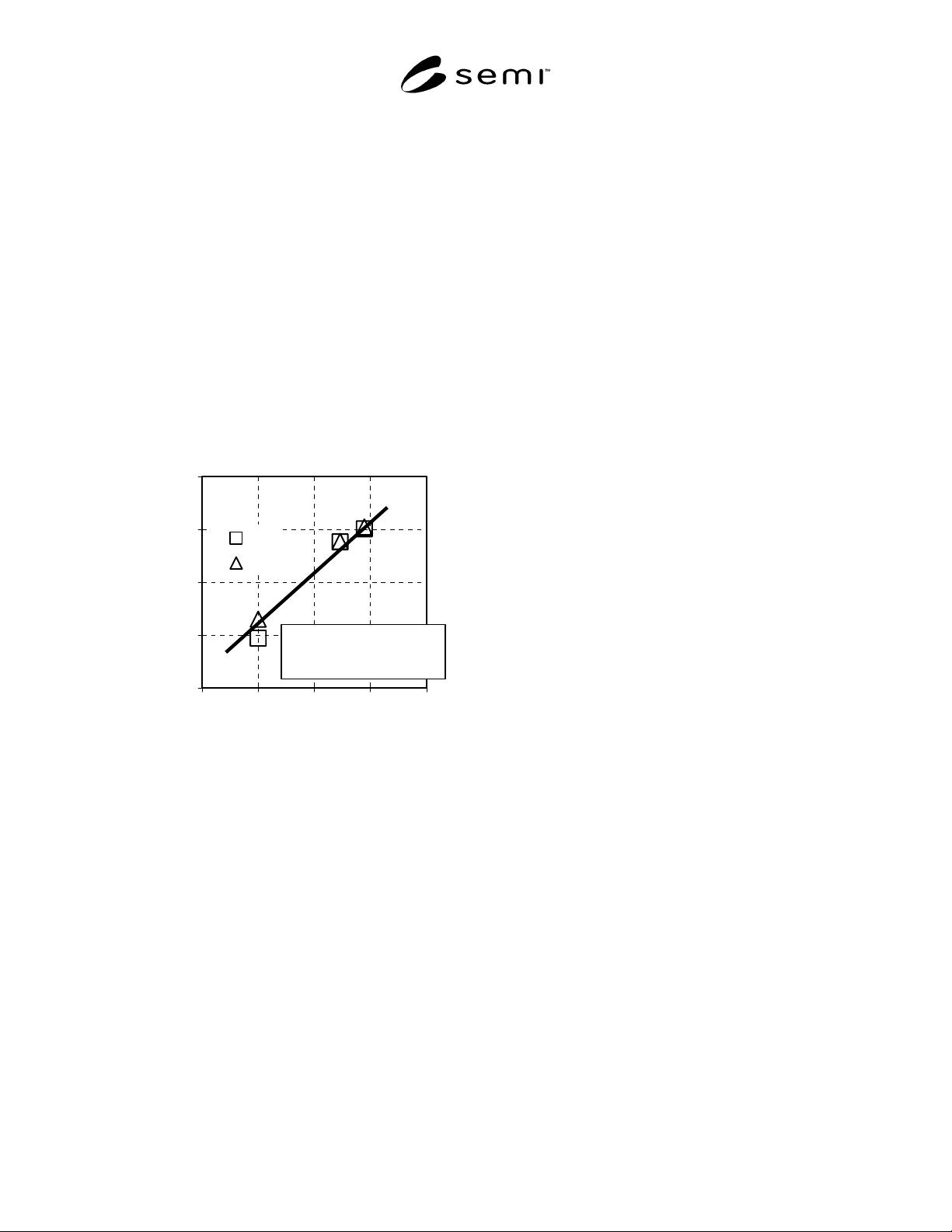
Figure R1-1
The Relationship between B-Mode Defect Density by
TZDB and OPP
R1-1.1.2 The above graph shows the relationship
between the B-mode defect density of 25 nm thick
oxide by TZDB and the particles by optical precipitate
profiler (OPP). Here, based on an assumption that the
dielectric breakdown defect is in conformance with the
Poisson distribution, the defect density by TZDB of 25
nm thick oxide, ρ, was calculated from the dielectric
breakdown failure fraction of TZDB, F, as follows.
ρ
ox
= -ln(1 – F)/S (8)
Here, S is a gate electrode area of the evaluated MOS
capacitors.
R1-1.1.3 The defect density was obtained by the B-
mode failure percent, F, of TZDB. On the other hand,
estimation of the defect density by OPP was carried out
as follows. The OPP defects were measured in the
wafers at the same position (ingot) of the same Si
crystal as the sample wafers. The density of COPs
which appeared on the silicon wafer surface was
estimated from the volume defect density, n(cm
-3
), and
the COP diameter, L(cm). The area density of the
defects which appear at the silicon surface can be
estimated with n × L, assuming that the COP diameter,
L, is almost uniform and the volume defect density, n,
is uniformly distributed. Here, 0.1 µm was used as the
L value
7
and the measurement results of the OPP
technique as the n value. The resulting OPP defect
densities, by which each of the three kinds of silicon
wafers, H, M, and L, was characterized, were as
follows.
H: n = 7.83 × 10
5
(cm
-3
) ⇒ ρ
ox
= 7.8(cm
-2
)
M: n = 2.89 × 10
5
(cm
-3
) ⇒ ρ
ox
= 2.9(cm
-2
)
L: n ≤ 1 × 10
4
(cm
-3
) ⇒ ρ
ox
≤ 0.1(cm
-2
)
In the above graph, C and G are the measurement
results for MOS capacitors made by two different wafer
vendors. The defect density by TZDB and the defect
density by OPP can be seen to be in a relation of almost
1:1 in this figure. These facts mean that the B mode
failure of the 25 nm thick gate oxide is mainly
attributable to the COPs that appear at the silicon wafer
surface. Moreover, these results indicate that this
standard test method can give us an evaluation of the
oxide defect densities over the wide range of COP
defect density with excellent reproducibility.
R1-1.2 Total Number and Electrode Area of Measured
MOS Capacitors
R1-1.2.1 To measure the defect density with a high
degree of accuracy, a large number of MOS capacitors
with a large electrode area shall be measured.
However, measurement of too large an area or too
many MOS capacitors leads to unnecessary evaluation
load. The appropriate area size and the total number of
MOS capacitors needed to evaluate the defect density at
the silicon wafer surface shall be selected according to
the foreseen defect density and the purpose of the
evaluation. For instance, if the purpose is to evaluate a
conventional, mirror-polished, CZ silicon wafer with a
defect density of 1–10/cm
2
, about 100 MOS capacitors
with an electrode area of 10–20 mm
2
must be measured.
R1-1.2.2 When the Poisson's distribution is assumed as
a defect distribution, as mentioned above, the yield, Y,
SEMI M51-0303 © SEMI 2002, 2003 12
of MOS capacitors with an electrode area of S and a
defect density of ρ
ox
is given by the following equation.
Y = 1 – F = exp(-ρ
ox
S)
R1-1.2.3 The failure fraction, F, is calculated using this
expression. Here, the necessary MOS capacitor
number, n, for the observation of one breakdown MOS
capacitor is assumed to be 1/F. Thus, this n was
calculated from the value of S and ρ
ox
as shown in
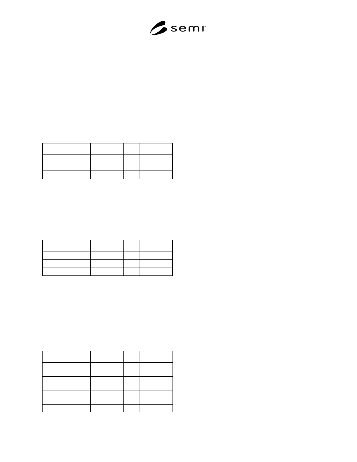
Table R1-1.
Table R1-1 Necessary number for observation of
one breakdown MOS capacitor
1/F = Necessary number for observation of one breakdown
MOS capacitor
S (mm
2
) 1 5 10 20 50
ρ
ox
= 10 cm
-2
11 3 2 1 1
ρ
ox
= 1 cm
-2
101 21 11 6 3
ρ
ox
= 0.1 cm
-2
1001 201 101 51 21
R1-1.2.4 In the same way, the yield probability, Y, and
necessary number, n, for observation of available MOS
capacitors was calculated as indicated in Table R1-2.
Table R1-2 Necessary number for observation of
available MOS capacitors
1/Y = Necessary number for observation of available MOS
capacitors
S (mm
2
) 1 5 10 20 50
ρ
ox
= 10 cm
-2
1 2 3 7 148
ρ
ox
= 1 cm
-2
1 1 1 1 2
ρ
ox
= 0.1 cm
-2
1 1 1 1 1
R1-1.2.5 The number of needed MOS capacitors is
shown in Table R1-3 though both “1/F” and “1/Y” were
done to one or more. To observe ten MOS capacitors
or more respectively in an actual evaluation including
reproducibility, the number of MOS capacitors required
for the measurement will then be multiplied by ten and
reaches the value shown in Table R1-3 below.
Table R1-3 Necessary number of MOS capacitors
(in the case of
ρ
ox
= 1 or 10)
S (mm
2
) 1 5 10 20 50
Confirmation of
breakdown (ρ
ox
= 1)
101 21 11 6 3
Confirmation of alive
(ρ
ox
= 10)
1 2 3 7 148
Necessary number
(large one in above)
101 21 11 7 148
×10 1010 210 110 70 1480
R1-1.2.5.2 In Table R1-3, the term confirmation of
breakdown (ρ
ox
= 1) means the number of elements
necessary to confirm at least one breakdown in the case
of ρ
ox
= 1, and the term of confirmation of alive
(ρ
ox
= 10) means the number of elements necessary to
confirm at least one alive in the case of ρ
ox
= 10.
R1-1.2.6 When a silicon wafer with a surface defect
density of 10/cm
2
is measured, if MOS capacitors with
an electrode area of 50 mm
2
are used, it breaks down.
Therefore, it is unsuitable for the comparative
evaluation of the defect distribution as in this test.
R1-1.2.7 To confirm that 10 MOS capacitors are
“alive” or “dead”, it is necessary to measure 70 MOS
capacitors with an electrode area of 20 mm
2
, or 110
MOS capacitors of 10 mm
2
, or 210 MOS capacitors of
5 mm
2
.
R1-1.2.8 When the defect density of a sample wafer is
0.1/cm
2
, we can confirm broken 10 MOS capacitors of
50 mm
2
by measurement of only 210 MOS capacitors.
For MOS capacitors of 1 mm
2
, it will be necessary to
measure about 10,000, and this is not realistic.
R1-1.3 Recommended Measurement Condition
R1-1.3.1 The electric field step, E
step
, and hold time,
T
hold
, used in this round robin are shown in Figure R1-2.
R1-1.3.2 In TZDB measurement, the voltage is
increased with each step. Then, the electric current is
measured after a constant hold time. This hold time is
usually initiated as a time period required for
measurement stabilization. It is possible that
measurement results are influenced by voltage
instability when the hold time is shorter than 100 ms.
R1-1.3.3 On the other hand, because too long a hold
time––that is, 800 ms or more––leads to a long total
measurement time, the influence of TDDB becomes
conspicuous in the high electrical field region, and it is
possible that the breakdown failure fraction of the MOS
capacitors increases.
R1-1.3.4 In Figure R1-2, the B-mode failure percents
are shown as a function of the hold time of the applied
electric field stress with a step height of 0.25 MV/cm.
A hold time from 100 ms to 800 ms did not have any
particular influence in the measurement results of this
round robin. Thus, we have proposed 200 ms as a
practicable recommended hold time.
R1-1.3.5 In this TZDB measurement, the applied
electric field was increased each step directly after the
current measurement. Too low a step height of the
applied electric field, ∆E––that is, 0.1 MV/cm or less––
leads to an unnecessarily long measurement time, and
the influence of TDDB becomes conspicuous in the
high electrical field region.