semi合集-English.pdf - 第5019页
SEMI M18-0704 © SEMI 1990, 2004 5 H 0609 — Test Methods of Crystalline Defects in Silicon by Preferential Etch Techniques H 0611 — Methods of Measurem ent of Thickness, Taper, and Bow of Silicon Wafers H 0612 — Testing M…

SEMI M18-0704 © SEMI 1990, 2004 4
50433/1 — Determination of the Orientation of Single
Crystals by Means of X-Ray Diffraction
50433/2 — Determination of the Orientation of Single
Crystals by Means of Optical Reflection Figure
50433/3 — Determination of the Orientation of Single
Crystals by Means of Laue Back Scattering
50434 — Determination of Crystal Defects in
Monocrystalline Silicon Using Etching Techniques on
{111} and {100} Surfaces
50435 — Determination of the Radial Resistivity
Variation of Silicon or Germanium Slices by Means of
a Four-Point-DC-Probe
50436 — Measurement of Metallurgical Thicknes of
Epitaxial Layers of Silicon by the Stacking Fault
Method
50437 — Measuring the Thickness of Silicon Epitaxial
Layers of Silicon by Infrared Intereference Method
[F95]
50438/1 — Determination of Impurity Content in
Silicon by Infrared Absorption: Oxygen
50438/2 — Determination of Impurity Content in
Silicon by Infrared Absorption: Carbon
50439 — Determination of the Dopant Concentration
Profile of Single Crystalline Semiconductor Material by
Means of the Capacitance-Voltage Method and
Mercury Contact [F 1392, F 1393]
50438/3 — Determination of Impurity Content in
Silicon by Infrared Absorption: Boron and Phosphorus
50440/1 — Measurement of Recombination Carrier
Lifetime in Silicon Single Crystals by Means of
Photoconductive Decay Method; Measurement on Bar-
Shaped Test Samples [F28]
50441/1 — Determination of the Geometric
Dimensions of Semiconductor Slices: Measurement of
Thickness
50441/2 — Determination of the Geometric
Dimensions of Semiconductor Slices: Testing of Edge
Rounding
50441/3 — Measurement of the Geometric Dimensions
of Semiconductor Slices; Determination of Flatness
Deviation of Polished Slices by Means of Multiple
Beam Interference
50441/4 — Determination of the Geometrical
Dimensions of Semiconductor Slices: Diameter and
Flat Depth of Slices
50443/1 — Recognition of Defects and Inhomogenities
in Semiconductor Single Crystals by X-Ray
Topography: Silicon
50444 — Conversion Between Resistivity and Dopant
Density; Silicon [F723 (phosphorous and boron only)]
50445 — Contactless Determination of the Electrical
Resistivity of Semiconductor Wafers with the Eddy
Current Method
50446 — Determination of Defect Types and Defect
Densities of Silicon Epitaxial Wafers [no direct ASTM
equivalent, compare F 1726 and associated standards]
3.5 ISO Standards
4
ISO 4287/1 — Surface Roughness – Terminology –
Part 1: Surface and its Parameters
ISO 14644/1-7 — Clean Room and Associated
Controlled Environments
3.6 JEITA (formerly JEIDA) Standards
5
43 — Terminology of Silicon Wafer Flatness
53 — Test Method for Recombination Lifetime in
Silicon Wafers by Measurement of Photoconductivity
Decay by Microwave Reflectance
56 — Standard Test Method for Substitutional Atomic
Carbon Content of Silicon by Infrared Absorption
61— Standard Test Method for Interstitial Atomic
Oxygen Content of Silicon by Infrared Absorption
EM-3602 — Determining the Orientation of a
Semiconductor Silicon Single Crystal
EM-3501 — Standard Specification for Dimensional
Properties of Silicon Wafers with Specular Surface
EM-3505 — Height calibration in 1nm order for AFM
3.7 JIS Standards
6
NOTE 2: ASTM equivalents are given in square brackets
following the title.
H 0602 — Testing Method of Resistivity for Silicon
Crystals and Silicon Wafers with Four-Point Probe
H 0604 — Measurement of Minority Carrier Life Time
in Silicon by Photoconductive Decay Method [F 28]
H 0607 — Testing Methods for Conductivity Type of
Semiconductor Materials
4 International Organization for Standardization, ISO Central
Secretariat, 1, rue de Varembé, Case postale 56, CH-1211 Geneva 20,
Switzerland. Telephone: 41.22.749.01.11; Fax: 41.22.733.34.30
Website: www.iso.ch
5 Japanese Electronic and Information Technology Industries
Association, Tokyo Chamber of Commerce and Industry Bldg. 2-2,
Marunouchi 3-chome, Chiyoda-ku, Tokyo 100-0005, Japan. Website:
www.jeita.or.jp
6 Japanese Industrial Standards, Available through the Japanese
Standards Association, 1-24, Akasaka 4-Chome, Minato-ku, Tokyo
107-8440, Japan. Telephone: 81.3.3583.8005; Fax: 81.3.3586.2014
Website: www.jsa.or.jp
SEMI M18-0704 © SEMI 1990, 2004 5
H 0609 — Test Methods of Crystalline Defects in
Silicon by Preferential Etch Techniques
H 0611 — Methods of Measurement of Thickness,
Taper, and Bow of Silicon Wafers
H 0612 — Testing Method of Resistivity for Single
Crystal Silicon Wafers (with Four Point Probe) [F 84]
H 0614 — Visual Inspection for Silicon Wafers with
Specular Surfaces
Z 8741 — Method of Measurement for Specular
Glossiness
3.8 Other Standard
7
ANSI/ASME B46.1 — Surface Texture (Surface
Roughness, Waviness, and Lay)
NOTICE: Unless otherwise indicated, all documents
cited shall be the latest published versions.
4 Terminology
4.1 The items listed in the form are referenced and
defined in various documents. A reference for most
items in Parts 2 and 3 of the form is listed in Table 1.
The entries in the table are keyed to the form by item
number. Because terms related to epitaxial wafers with
buried layer are defined in this standard and because no
standardized test methods for the buried layer
parameters exist, Table 1 does not include line items
from Part 4 of the form.
4.2 General term used in this standard:
4.2.1 required (req. or req'd) — when applied to a
parameter listed in the order form, a user-supplied value
is necessary to minimally define the material for
manufacture.
4.3 Terms related to epitaxial wafers with buried
layers:
4.3.1 buried layer — a diffused region in a substrate
that is, or is intended to be, covered with an epitaxial
layer.
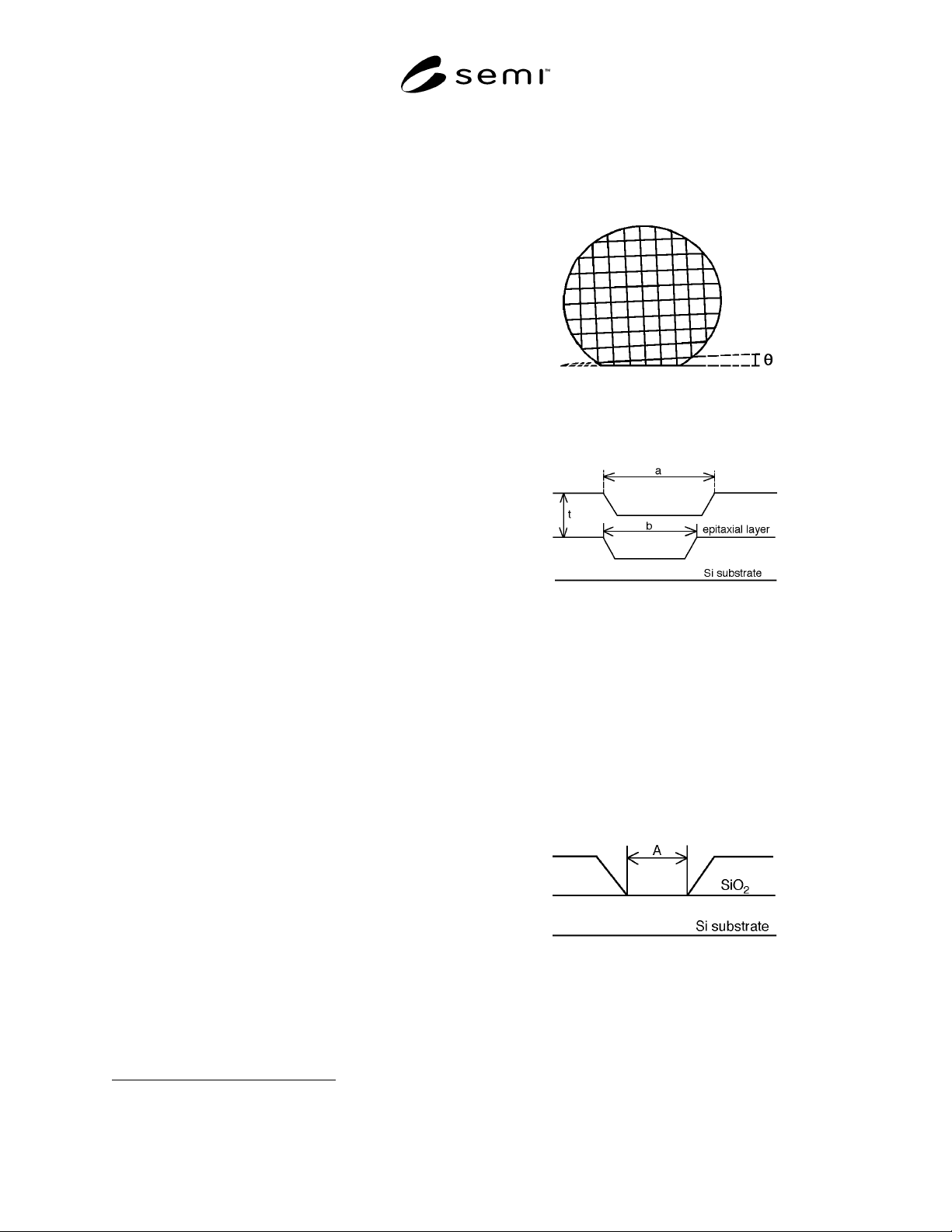
4.3.2 alignment precision — pattern displacement in
first mask photolithography process.
NOTE 3: Alignment precision is specified by maximum
values of X and Y, the displacement of the center of the
pattern from a reference position defined in the wafer
specification in terms of the wafer coordinate system defined
in SEMI M20, and the maximum value of θ, the angle
between the x-axis of the pattern and the primary orientation
flat (see Figure 1).
7 The Amercan Society of Mechanical Engineers, United Engineering
Center, 345 E. 47th St., New York, NY 10017.
4.3.3 pattern distortion ratio — absolute magnitude of
the quotient of the (1) difference between the width of
the pattern on the substrate and the width of the pattern
on the top surface of the epitaxial layer and (2) the
thickness of the epitaxial layer.
Figure 2
First Mask Showing Angular
Displacement
θ
Figure 3
Cross-Section View of Epitaxial Layer Showing the
Pattern Widths, a, at the Epi Surface, and b, at the
Layer-Substrate Interface
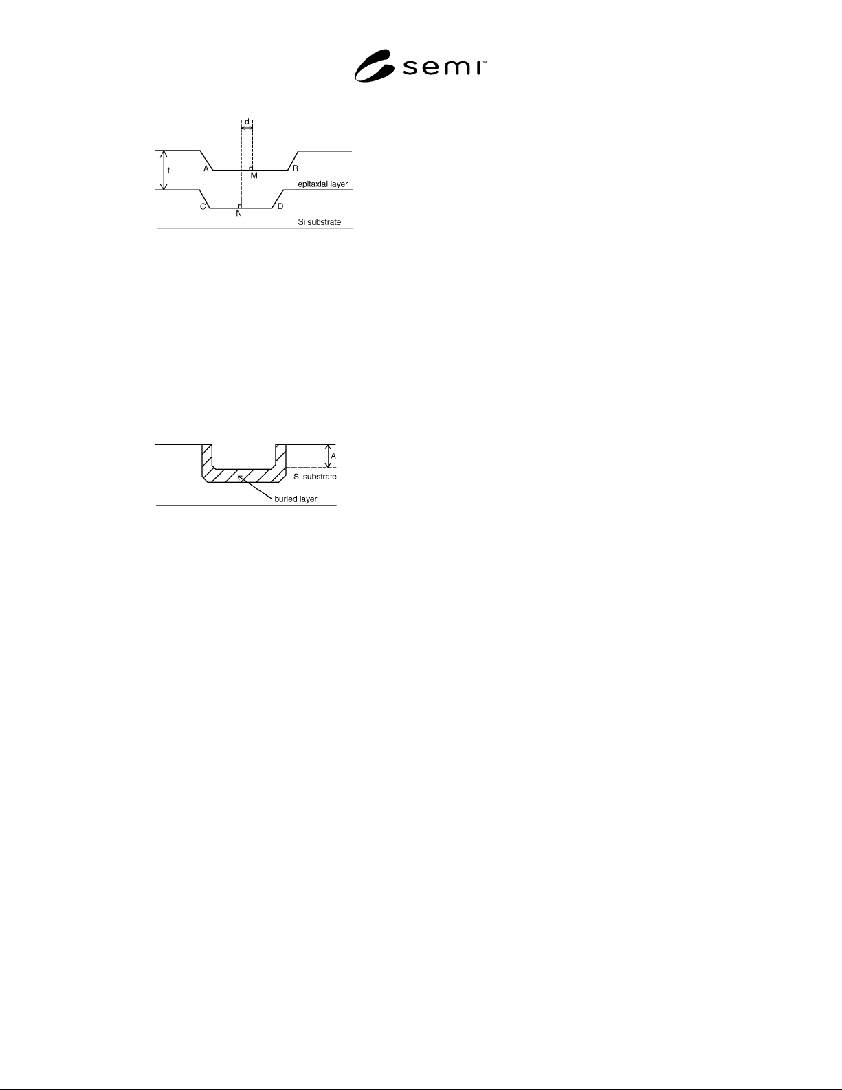
4.3.4 pattern shift ratio — lateral distance between the
center point of the pattern on the surface of the
substrate and the center point of the pattern on the
surface of the epitaxial layer divided by the epitaxial
layer thickness.
NOTE 4: Pattern shift ratio, d/t (see Figure 4), is specified in
terms of a nominal value, X, and a tolerance, ± Y, both of
which are dimensionless because both d and t are in µm.
Figure 4
Schematic Diagram Showing Line Width, A, of
Pattern on Substrate Wafer
SEMI M18-0704 © SEMI 1990, 2004 6
Figure 5
Cross-Section View of Epitaxial Wafer Showing the
Pattern Shift, d. Not to scale: AM = MB and CN =
ND
4.3.5 pattern step height — difference in vertical
position of the diffused (buried layer) surface and the
original substrate surface, after removal of oxide.
NOTE 5: Pattern step height, A, is specified as a nominal
value, X, and a tolerance ± Y, both in nm. See Figure 5.
Figure 6
Cross-Sectional View of Epitaxial Substrate After
Oxide Removal but Before Deposition of the
Epitaxial Layer Showing the Pattern Step Height, A
4.4 Terms Related to Annealed Wafers
4.4.1 annealed wafer — wafer that has defects (COP)
free zone near the surface produces by high temperature
annealing.
4.4.1.1 hydrogen annealed wafer — annealed wafer
produced under hydrogen atmosphere.
4.4.1.2 argon annealed wafer — annealed wafer
produced under argon atmosphere.
4.5 Terms Related to SOI Wafers
4.5.1 SOI wafer — wafer that has a buried oxide layer
(BOX).
4.5.1.1 SIMOX wafer — SOI wafer made by oxygen
implantation and high temperature annealing
technology.
4.5.1.2 Bonded wafer — SOI wafer made by bonding
two silicon wafers with an insulating layer between
them. The insulating layer is typically grown oxide.
5 Use of the Form
5.1 Different parts of the specification form are used
for ordering different types of silicon wafers:
5.1.1 For polished wafers, complete Parts 1 and 2.
5.1.2 For epitaxial wafers, complete Parts 1, 2, and 3.
5.1.3 For epitaxial wafers with buried layer, complete
Parts 1, 2, 3, and 4.
5.1.4 For annealed wafers, complete parts 1, 2, and 5.
5.1.5 For SOI wafers, complete Parts 1, 2, and 6. If
necessary, complete Parts 3, 4, or 5.
5.2 In all cases, items listed as required must have a
value or choice indicated to minimally specify the
material.
5.3 Certain required dimensional items may be
specified as a group according to the standard values
presented in the applicable SEMI specification, or they
may be specified individually.
5.4 Visual inspection criteria may be specified as a
group according to the standard values listed in the
applicable SEMI specification, or they may be specified
individually.
5.5 For either dimensional values or visual inspection
criteria, the appropriate SEMI specification may be
marked and an optional line item (or items) marked as
well. In this case, the value marked on each individual
line item takes precedence over the standard value.
5.6 If the suggested form included in this format is not
reproduced and used as a fill-out form, the items and
responses must be adequately identified so that the
information and requirements are clear to all parties.
6 Test Methods
6.1 Measurements shall be made or certifiable to the
ASTM, JEITA, JIS, or DIN standard test method as
cited in Table 1.
6.2 When standard test methods from different
geographic regions are available, the default method
shall be the method in common usage for the region of
the purchaser of the wafer.
6.3 If several different standard test methods for an
item are commonly used within a region, a specific
entry must be made to identify which method of test is
applicable.
6.4 If no standard test method for an item is available,
the test procedure must be specified.