semi合集-English.pdf - 第5809页
SEMI P23-0200 © SEMI 1993 , 2000 32 Figure 27 Sensitivity Check Sheet – Contact Hole Pa ttern NOTICE: SEMI makes no warranties or representations as to the su itability of the guideline set forth herein for any particula…
SEMI P23-0200 © SEMI 1993, 200031
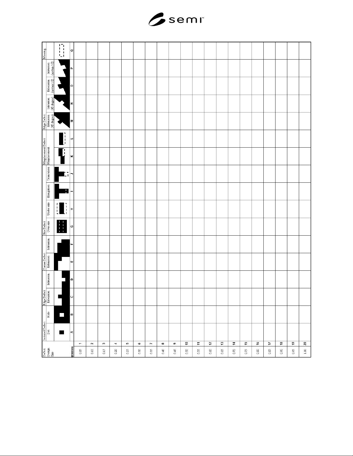
Figure 26
Sensitivity Check Sheet – Wiring Pattern
SEMI P23-0200 © SEMI 1993, 2000 32
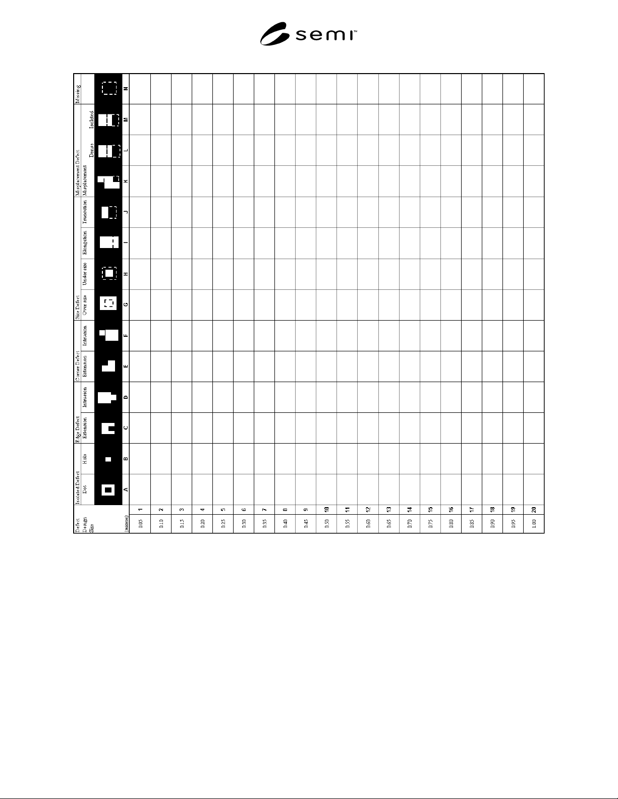
Figure 27
Sensitivity Check Sheet – Contact Hole Pattern
NOTICE: SEMI makes no warranties or representations as to the suitability of the guideline set forth herein for any
particular application. The determination of the suitability of the guideline is solely the responsibility of the user.
Users are cautioned to refer to manufacturer’s instructions, product labels, product data sheets, and other relevant
literature respecting any materials mentioned herein. These guidelines are subject to change without notice.
The user’s attention is called to the possibility that compliance with this guideline may require use of copyrighted
material or of an invention covered by patent rights. By publication of this guideline, SEMI takes no position
respecting the validity of any patent rights or copyrights asserted in connection with any item mentioned in this
guideline. Users of this guideline are expressly advised that determination of any such patent rights or copyrights,
and the risk of infringement of such rights, are entirely their own responsibility.
Copyright by SEMI® (Semiconductor Equipment and Materials
International), 3081 Zanker Road, San Jose, CA 95134. Reproduction o
f
the contents in whole or in part is forbidden without express written
consent of SEMI.

SEMI P24-94 © SEMI 1994, 2004 1
SEMI P24-94 (Reapproved 1104)
CD METROLOGY PROCEDURES
This standard was technically approved by the Global Micropatterning Committee and is the direct
responsibility of the North American Micropatterning Committee. Current edition approved by the North
American Regional Standards Committee on July 11, 2004. Initially available at www.semi.org September
2004; to be published November 2004. Originally published in 1994.
1 Purpose
1.1 The purpose of this document is to establish
uniform procedures for metrology systems for the litho-
metrology task. It does not address how these systems
will be applied to solve problems, nor does it address
other contributors to process variations such as thermal
wafer processing, exposure tool focus control,
materials, etc.
1.2 Background — Fundamental to manufacturing is
the gauging or measurement process. It is required
initially to develop a usable manufacturing capability
and then to verify that what is being manufactured
conforms to specification/expectation.
2 Scope
2.1 This document discusses determining the
performance of gauging/measurement systems for a
very specific application — the lithography section of
integrated circuit wafer fabrication. This document in
many cases, will be applicable to IC mask-making, in
which case the word “mask” can be substituted for
“wafer.”
2.2 It is acknowledged that the final measurement for a
fabricated wafer is the electrical functionality.
However, the intermediate lithographic measurements
can be useful in prediction and control of final
functionality. This document is intended to be useful
for this litho-metrology application, irrespective of the
technology employed.
2.3 Measurement results and system performance
depend on the sample(s) used. Therefore, performance
for different systems or the same system at different
times can only be appropriately compared when the
measurements are obtained with a sample of the same
material composition.
2.4 The parameter addressed is precision. Additional
important parameters are reliability and cleanliness,
which have been addressed by other SEMI standards.
NOTICE: This standard does not purport to address
safety issues, if any, associated with its use. It is the
responsibility of the users of this standard to establish
appropriate safety and health practices and determine
the applicability of regulatory or other limitations prior
to use.
3 Referenced Standards
3.1 SEMI Standards
SEMI E10 — Standard for Definition and Measurement
of Equipment Reliability, Availability, and
Maintainability (RAM)
SEMI P19 — Specification for Metrology Pattern Cells
for Integrated Circuit Manufacture
3.2 ASTM Standards
1
ASTM D 1129 — Standard Terminology Relating to
Water
ASTM C 609 — Standard Test Method for
Measurement of Small Color Differences Between
Ceramic Wall or Floor Tile
ASTM D 4790 — Standard Terminology of Aromatic
Hydrocarbons and Related Chemicals
ASTM E 180 — Standard Practice for Determining the
Precision of ASTM Methods for Analysis and Testing
of Industrial and Specialty Chemicals
NOTICE: Unless otherwise indicated, all documents
cited shall be the latest published versions.
4 Applications
4.1 linewidth measurement — this task is to measure
linewidths as defined by SEMI P19.
NOTE 1: Pitch is not addressed in this document.
4.2 contact hole measurement — contact and via hole
area measurement is a different application which may
use the same definitions and procedures as line-width
measurement.
1 American Society for Testing and Materials, 100 Barr Harbor
Drive, PO Box C700, West Conshohocken, PA, 19428-2959, Phone:
(610) 832-9585, Fax: (610) 832-9555, http://www.astm.org/