semi合集-English.pdf - 第5111页
SEMI M24-1103 © SEMI 1994, 2003 14 NOTE 1: Nominal Edge Exclusion is proposed as the same as in Ta ble2 and as in Table3, however, more discussion will be necessar y. Edge Exclusion Task Force is now making activitie s f…
SEMI M24-1103 © SEMI 1994, 2003 13
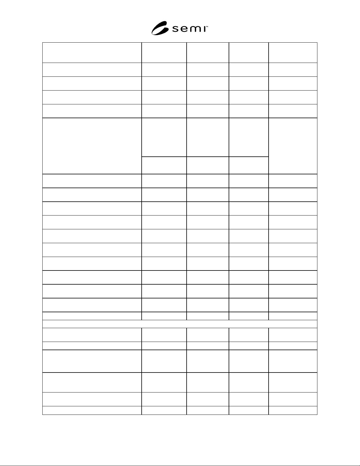
CLASSIFICATION ITEMS (SEMI M18) Particle Counting
Furnace &
Thermal Process
Lithography &
Patterning
Test Method
8.1 A Scratches, Macro (See Note 5.) None None None ASTM F 154, F 523,
JIS H 614
8.1 B Scratches, Micro (See Note 5.) None
≤ 1/10 × D mm ≤ 1/10 × D mm
ASTM F 154,
JIS H 614
8.2 Pits None None None ASTM F 154, F 523,
JIS H 614
8.3 Haze (See Note 5.) None None None ASTM F 154, F 523,
JIS H 614
≤ 60/wf
≤ 27/wf
NS
NS
NS
NS
8.4 Localized Light Scatterers
(Particulate 90 nm Contamination; LLSs)
(See Note 6.)
300 mm
200 mm
(Particulate 0.13 µm Contamination; LLSs)
(See Note 7.)
-
≤ 0.15/cm
2
≤ 0.15/cm
2
SEMI M25,
ASTM F 523,
F 1620, F 1621
8.5 Contamination/Area None None None ASTM F 154, F 523,
JIS H 614
8.6 Edge chips None None None ASTM F 154, F 523,
JIS H 614
8.7 Cracks, Crow’s Feet None None None ASTM F 154, F 523,
JIS H 614
8.8 Craters None None None ASTM F 154, F 523,
JIS H 614
8.9 Dimples None None None ASTM F 154, F 523,
JIS H 614
8.10 Grooves None None None ASTM F 154, F 523,
JIS H 614
8.11 Mounds None None None ASTM F 154, F 523,
JIS H 614
8.12 Orange Peel None None None ASTM F 154, F 523,
JIS H 614
8.14 Saw Marks None None None ASTM F 154, F 523,
JIS H 614
8.15 Dopant Striation Ring None None None ASTM F 154, F 523,
JIS H 614
8.- Microroughness NS NS NS
9. BACK SURFACE VISUAL INSPECTION CHARACTERISTICS
9.1 Edge Chips None None None ASTM F 154, F 523,
JIS H 614
9.6 Roughness, rms NS NS NS
9.7 Brightness (Gloss)
300 mm
200 mm
≥ 80%
User/Vendor
≥ 80%
User/Vendor
≥ 80%
User/Vendor
ASTM D 523,
JIS Z8741
9.8 Localized Light Scatterers (LLSs) NS NS NS ASTM F 523,
F 1620, F 1621,
JIS H 614
9.9 Scratches, Macro
≤ 0.25 × D mm ≤ 0.25 × D mm ≤ 0.25 × D mm
ASTM F 154, F 523,
JIS H 614
9.10 Scratches, Micro NS NS NS ASTM F 154
SEMI M24-1103 © SEMI 1994, 2003 14
NOTE 1: Nominal Edge Exclusion is proposed as the same as in Table2 and as in Table3, however, more discussion will be necessary. Edge
Exclusion Task Force is now making activities for developing a guide containing definition of edge exclusion when a measurement is made over
a finite sampling area.
NOTE 2: Wafer ID Marking: SEMI M1 specification shall be applied, if ID mark is applied.
NOTE 3: Surface Metal Contamination for Furnace and Thermal Process: The specification values are based on ITRS ’99 Roadmap.
NOTE 4: Surface Metal Contamination for Particle Counting and Lithography & Patterning: The specified values are based on 180 nm process
requirement in ITRS 1999.
NOTE 5: Visual techniques are neither sufficient nor appropriate for 0.13 µm design rules. Automatic surface inspection tools can be used for
reporting values such as scratches and haze. Test method and standardization for automatic surface inspection tools is under development, visual
inspection is now used as a supplemental method.
NOTE 6: LLSs (Localized Light Scatterers: 90 nm): These specification values shall be reviewed when the evaluation techniques for
distinguishing particle and COP are established. Critical surface LLS size should be the half of CD, however, tools are not well established. 65
nm count limit was transferred to 90 nm count limit using draft international standard: ISO/DIS 14644-1 which follows the equation: 90 nm LLS
counts per wafer = 65 nm LLS counts per wafer /(90 nm /65 nm)
2
.
NOTE 7: LLSs for Furnace & Thermal Process and Lithography & Patterning: New concept is proposed for LLSs for Furnace and Thermal
Process. The critical surface LLS size for prime wafer is proposed as a half size of CD in IRTS Roadmap. The half of CD is not necessarily
requested for monitor test wafers. In actual business, an additional specification of LLS, the size of which is around CD is used, however, the size
is not standardized. TF proposes the additional LLS size as the same size as CD. This size is used for specifying LLS for Furnace & Thermal
Process.
NOTE 8: ASTM F47-94 (Discontinued 1998) was replaced by ASTM Guide F1725, and ASTM F416-94 (Discontinued 1998) was replaced by
ASTM Practice F1727.
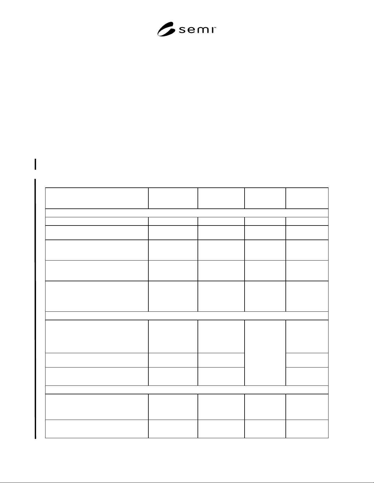
Table 5 Specification for Polished Monocrystalline Silicon Premium Wafers for 90 nm Design Rule Usage
CLASSIFICATION ITEMS (SEMI M18) Particle Counting
Furnace & Thermal
Process
Lithography &
Patterning
Test Method
1. GENERAL CHARACTERISTICS
1.1 Growth Method Cz or MCz Cz or MCz Cz or MCz
1.2. Crystal Orientation (100) (100) (100) ASTM F 26,
DIN 50433
1.3 Conductivity Type n or p n or p n or p ASTM F 42,
JIS H607
DIN 50432
1.4 Dopant P or B P or B P or B ASTM F 1389,
F 1630, DIN
50438/3
1.5 Nominal Edge Exclusion (See Note 1.)
(Fixed Quality Area)
300 mm
200 mm
2 mm
2 mm
2 mm
2 mm
2 mm
2 mm
2. ELECTRICAL CHARACTERISTICS
2.1 Resistivity, Center Point NS
≥ 1 Ω•cm
ASTM F 84, F
673,
JIS H 602,
DIN 50431,
50445
2.2 Radial Resistivity Variation NS NS ASTM F 81,
DIN 50435
2.4 Minority Carrier Lifetime
(Carrier Recombination Lifetime)
NS
≥ 325 µs
NS
JEIDA 53,
ASTM F 1535
3. CHEMICAL CHARACTERISTICS
3.1 Oxygen Concentration NS
≤ 1.2 × 10
18
/cm
3
NS ASTM F 1188,
F 1619
DIN 50438/1
3.1.1 Oxygen Concentration Tolerance:
Tolerance around Center Point
≤ 10%
SEMI M24-1103 © SEMI 1994, 2003 15
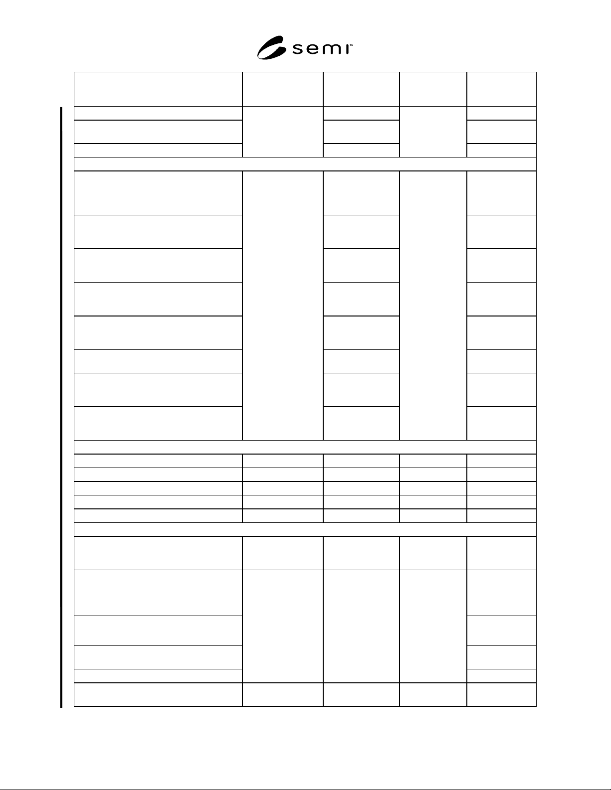
CLASSIFICATION ITEMS (SEMI M18) Particle Counting
Furnace & Thermal
Process
Lithography &
Patterning
Test Method
3.2 Radial Oxygen Variation NS
3.3 Carbon Concentration ≤ 0.2 ppma ASTM F 1391,
DIN 50438/2
3.- Total Bulk Iron Concentration
≤ 5 × 10
10
/cm
3
ASTM F 978
4. STRUCTURAL CHARACTERISTICS (See Note 2.)
4.1 Dislocation Etch Pit Density ≤ 500/cm
2
ASTM F 1725,
JIS H 609,
DIN 50434,
50443/1
4.2 Slip None ASTM F 1725
JIS H 609, DIN
50434, 50443/1
4.3 Lineage None ASTM F 1725,
JIS H 609, DIN
50434, 50443/1
4.4 Twin None ASTM F 1725,
JIS H 609, DIN
50434, 50443/1
4.5 Swirl None ASTM F 1727,
JIS H 614,
DIN 50443/1
4.6 S-pits None ASTM F 1727,
F 1049
4.7 Oxidation Induced Stacking Faults (OSF) User/Vendor ASTM F 1727,
User/Vendor
mutual agreement
4.8 Oxide Precipitates (BMD)
Interstitial Oxygen Reduction (∆ Oi)
NS
User/Vendor
NS
ASTM F 1239,
User/Vendor
mutual agreement
5.WAFER PREPARATION CHARACTERISTICS
5.1 Wafer ID Marking (See Note 3.) Optional Optional Optional
5.3 Denuded Zone NS NS NS
5.4 Extrinsic Gettering Treatment None None None
5.5 Backseal NS None NS
5.6 Annealing NS Donor Annih. Only NS
6. MECHANICAL CHARACTERISTCS
6.1 Diameter 200 and 300 mm 200 and 300 mm 200 and 300 mm ASTM F 613,
DIN 50441/4,
JEIDA27
6.2 Primary Flat Length/Diameter
Notch Dimensions
ASTM F 671,
F 1152, DIN
50441/4
JEIDA 27,
6.3 Primary Flat/
Notch Orientation
ASTM F 847
6.4 Secondary Flat Length ASTM F 671,
DIN 50441/4
6.5 Secondary Flat Location
SEMI M1 SEMI M1 SEMI M1
ASTM F 847
6.6 Edge Profile SEMI M1 SEMI M1 SEMI M1 ASTM F 928,
DIN 50441/2