semi合集-English.pdf - 第7866页
SEMI T13-1104 © SEMI 2004 26 RELATED INFORMATION 1 DEVICE TRACKING EXAMPLES NOTICE : This related information is not an official pa rt of SEMI T13 and was derived from the Japanese Traceability Committee. This related in…

SEMI T13-1104 © SEMI 2004 25
APPENDIX 2
COORDINATE SYSTEMS
NOTICE: The material in this appendix is an official part of SEMI T13 and was approved by full letter ballot
procedures on April 30, 2004.
A2-1 Horizontal Coordinates
A2-1.1 Die Coordinate, Origin and Fiducial — Definition of the origin of coordinates used with this specification
is basically compliant to such SEMI standard as G81 and G84. For complicated or irregular die arrangement
including sub-array of dice, it is assumed to be compliant to Section 18 Coordinate System in SEMI E130. If the
other coordinate system or origin definitions, which are specific to substrates or user/equipment dependent, user or
supplier shall specify in specification or complementary document. Fiducial information shall be also documented if
it is necessary for tracking.
A2-1.2 The other Coordinate Systems — If surface position is required to give Die Trace Data except Device
coordinates, such SEMI standard as M17, M20 or M21 shall be basically used: e.g. for visual inspection and film
thickness measurement. If some derivations from the standards or complete different coordinate system are required,
depending on equipment, supplier or user shall document to exchange specification.
A2-2 Vertical Dimension
A2-2.1 Vertical Position — Sometimes vertical position may be required to represent Die Trace Data. This standard
assumes one of the following representation of vertical position.
A2-2.1.1 Z Dimension — This representation consists of ‘Order’ and ‘Height’. ‘Order’ means order number of
concerning device from lowest substrate. ‘Height’ is actual vertical dimension of concerning device from top surface
of the device just below it or substrate. Unit of the Height is given with the value or common with the other
information. See R1-3 for example.
A2-2.1.2 GCD Grid — When above positioning system is not convenient or doesn’t work for specific equipment or
tracking system, this system is used alternatively. Take Greatest Common Denominator (GCD) of all mounted
devices on substrate and assume a grid of the GCD. It may be 50 micron for example. The origin of the grid must be
surface of base substrate and minus vale may be used in such a case that a die is implanted in the substrate. This may
be useful for some advanced assembly or bird-eye view preferred systems.
A2-2.2 The Other Vertical dimensions — Additional vertical dimension may be required for some equipment.
Because they are equipment dependent, this document doesn’t specify anything about coordinates except the
previous subsections. User or suppliers shall document to understand Die Trace Data correctly.
SEMI T13-1104 © SEMI 2004 26
RELATED INFORMATION 1
DEVICE TRACKING EXAMPLES
NOTICE: This related information is not an official part of SEMI T13 and was derived from the Japanese
Traceability Committee. This related information was approved for publication by full letter ballot on April 30,
2004.
R1-1 Device Tracking Report
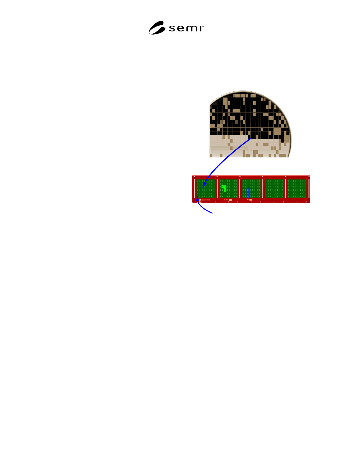
R1-1.1 The following figurer and list are example of
Device Tracking Report.
R1-1.1.1 Device Example — The following Figure
shows a device picked from a wafer and placed on a
strip.
R1-1.1.2 Report Example — The following list shows
an example of the report for the first 2 devices on a strip
taken from Wafer1 and the next 2 taken from Wafer2.
From Substrate
OriginLocation(0,0) = "LowerLeftTop"
RowColumnMajor = "Column"
FromX
FromY
To Substrate
Index = 15
Rows = 6
Columns = 40
ToX = 2
ToY = 4
Figure R1-1
SEMI T13-1104 © SEMI 2004 27
List 1 An Example of Device Tracking Data in XML
<?xml version="1.0" encoding="utf-8" ?>
<
DeviceTrackingData xmlns="urn:semi-org:xsd.Doc3754.V0312.DeviceTrackingData">
<SubstrateType>Strip</SubstrateType>
<SubstrateId>MyStrip</SubstrateId>
<LayoutId>Device</LayoutId>
<OriginLocation>LowerLeftTop</OriginLocation>
<RowColumnMajor>Column</RowColumnMajor>
<FromSubstrate>
<SubstrateType>Wafer</SubstrateType>
<SubstrateId>Wafer1</SubstrateId>
<D><X>10</X><Y>18</Y></D>
<D><X>7</
X><Y>17</Y></D>
</FromSubstrate>
<FromSubstrate>
<SubstrateType>Wafer</SubstrateType>
<SubstrateId>Wafer2</SubstrateId>
<D><X>18</X><Y>1</Y></D>
<D><X>9</X><Y>0</Y></D>
</FromSubstrate>
</
DeviceTrackingData>
NOTE 1: The <D> elements contain the X and Y location on the substrate from which they came.
NOTE 2: The <FromSubstrate> element specifies the substrate type and identifier from which the devices came from.
NOTE 3: The <D> elements represent each device on the layout “Device” for strip “MyStrip”.
NOTE 4: The number of <D> entries must equal Rows * Columns defined in the “Device” layout.
NOTE 5: The one dimensional array of <D> elements represents the two dimensional array of locations defined in the “Devices” layout in
RowColumnMajor format with respect to the OriginLocation.
NOTE 6: The OriginLocation corresponds to the definition of the same name in SEMI G81.
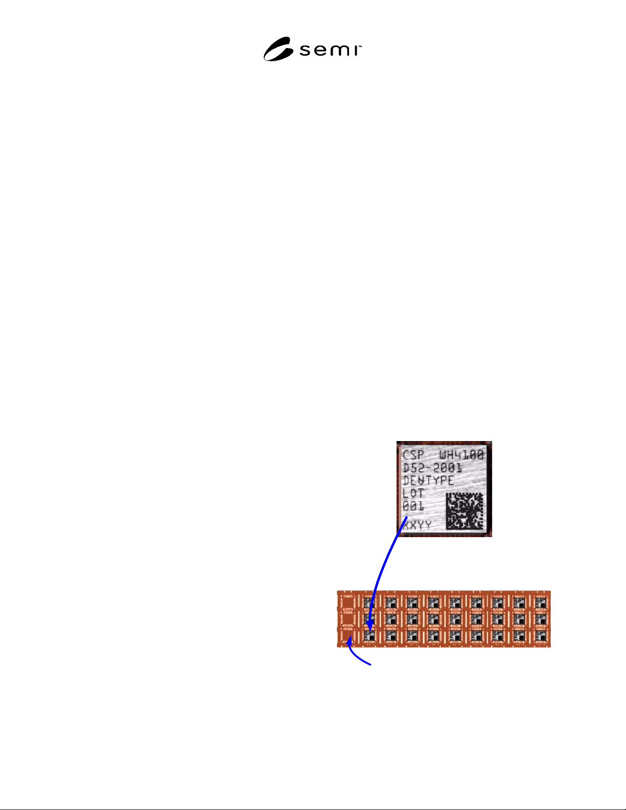
R1-2 Device ID Report
R1-2.1 ID Example — The following figure shows a
strip of devices with alphanumeric and 2D matrix
marks. The unique part of the 2D mark is “LOT001-
XXYY”.
R1-2.2 Report Example — The following list shows a
truncated version of the Device Id Data report for the
strip shown in upper figure.
Substrate
Index = 3
Rows = 3
Columns = 10
ToX = 1
ToY = 1
OriginLocation (0,0) ="LowerLeftTop"
RowColumnMajor="Column"
DeviceId
Figure R1-2