semi合集-English.pdf - 第5418页
SEMI M58-0704 © SEMI 2004 11 Lab: Company ABC Identification of deposition system used: 1 Contact N . P. Teste r Supplier/Model # Dep Sys/45U 2 Address 456 Main Street Syste m S/N 12345 3 Anywhere, CA, U SA Syste m S/W R…

SEMI M58-0704 © SEMI 2004 10
R2-3.5 Interpretation of Results
R2-3.5.1 A conditional command is used to
automatically grade results for Uncertainty and FWHM.
R2-3.5.1.1 The equation for Bottle B Uncertainty (row
50) is: =IF(J34>0.03," Fail" ," Pass" ), and the others are
similar.
R2-3.5.1.2 The equation for Bottle B FWHM (row 51)
is =IF(J35>0.05," Fail" ," Pass" ), and the others are
similar.
R2-3.5.2 These are the only two requirements of SEMI
M52 verified by this test method. Two additional
comparisons are made for information only:
R2-3.5.2.1 The SSIS Peak diameter is compared with
the corrected deposition system peak diameter (row 52).
For Bottle B the equation is =B52/J37, and the others
are similar.
R2-3.5.3 Finally, the SSIS mean count is compared
with the count from the deposition system (row 53).
The equation for Bottle B is =E52/$ D$ 13, and the
others are similar.
SEMI M58-0704 © SEMI 2004 11
Lab: Company ABC Identification of deposition system used:
1
Contact
N
. P. Teste
r
Supplier/Model # Dep Sys/45U
2
Address
456 Main Street System S/N 12345
3
Anywhere, CA, USA System S/W Revision 3
4
Phone
782-555-5555 Date of Test
5
email nptester@abcco.com
Date of Last Previous Test
N
ot applicable
6
7
Characteristics of Suspensions Used for Test
8
u
B
ottle i
%FWHM
i
9
B
ottle A, Certified
100.7 nm ± 0.5
nm (1
σ
) or
0.5% 2.0%
10
79 nm ± 2.6
nm (1
σ
) or
3.3% 10.0%
11
145 nm ± nominal
nm (1
σ
) or
not available unknown
12
Particles Deposited (
N
)
3000
13
S
upplier
P
art No.
L
ot No.
14
Deposition System Diameters (nm)
B
ottle A
N
IST SRM 1963 ? ?
15
B
ottle A
B
ottle B
B
ottle
C
B
ottle A
B
ottle B ? ? ? ? ? ?
16
D
ay
nm nm nm nm
B
ottle
C
? ? ? ? ? ?
17
1
101.5 79.6 155.6 101.0
18
2
100.5 79.0 153.9 101.0
19
3
101.0 78.2 154.6 102.0 SSIS Data: Bottle C
20
4
102.0 78.5 155.9 102.0
21
5
101.0 78.1 154.3 102.0
22
M
ean
101.2 78.7 154.9 101.6
D
ay
nm nm %
23
s
D
ep
0.6% 0.8% 0.6% 0.5%
1
149.2 3.3 2.21% 2815
24
2
148.9 3.6 2.42% 2548
25
Dep System Sizing Corrections
3
150.9 3.4 2.25% 2720
26
M
ean
A
=
101.4 nm
4
151.1 3.6 2.38% 2716
27
s
D
epA
=
0.6%
5
149.7 3.4 2.27% 2178
28
Cert
A
−
Mean
A
=
-0.7 nm
M
ean
150.0 3.5 2.31% 2595
29
Std Dev 0.994 0.134 0.088%
252.4
30
SSIS Data: Bottle A
31
Analysis
32
B
ottle A
B
ottle B
B
ottle
C
33
D
ay
nm nm %
D
ep Peak Uncertainty
1.5% 1.9% 1.5%
34
1
95.6 2.1 2.20% 2178
F
WHM (SSIS)
2.3% 3.3% 2.3%
35
2
95.9 2.2 2.29% 2418
P
eak (Dep System)
101.4 78.7 154.9
36
3
96.1 2.3 2.39% 2555
P
eak (Dep Sys Corrected)
100.7 78.1 153.8
37
4
96.1 2.2 2.29% 2512
P
eak (SSIS)
96 72 150
38
5
96.2 2.2 2.29% 1929
M
easured Count
2318 2524 2595
39
M
ean
96.0 2.2 2.29% 2318
40
Std Dev 0.239 0.071 0.070% 262.1
Compare Quantity with Limit
41
42
SSIS Data: Bottle B
Uncertainty Limit
43
F
WHM Limi
t
44
SSIS Peak
45
D
ay
nm nm %
SSIS Count
46
1
72.6 2.4 3.31% 2297
47
2
71.6 2.3 3.21% 2690 Interpretation of Results
48
3
72.2 2.3 3.19% 2742
B
ottle A
B
ottle B
B
ottle
C
49
4
72.2 2.3 3.19% 2735
Uncertainty
Pass Pass Pass
50
5
71.2 2.5 3.51% 2156 Pass Pass Pass
51
M
ean
72.0 2.4 3.28% 2524
SSIS/Dep Peak Comp
0.95 0.92 0.98
52
Std Dev 0.555 0.089 0.138%
276.8
SSIS/Dep Count Comp
0.77 0.84 0.87
53
A B C D E F G H I J K
August 20, 2003
B
ottle B
B
ottle
C
S
uspension
P
ea
k
Diameter
M
easured
Peak
F
WHM
on Wafer
R
elative
F
WHM
Count
F
WHM
Dep Sys Corrected Peak (Info only)
5.0% (SEMI M52)
3.0% (SEMI M52)
Dep System Count (Info only)
Count
L
imi
t
F
WHM
on Wafer
M
easured
Peak
R
elative
F
WHM
Quantity
Count
R
elative
F
WHM
M
easured Pea
k
F
WHM on
Wafer
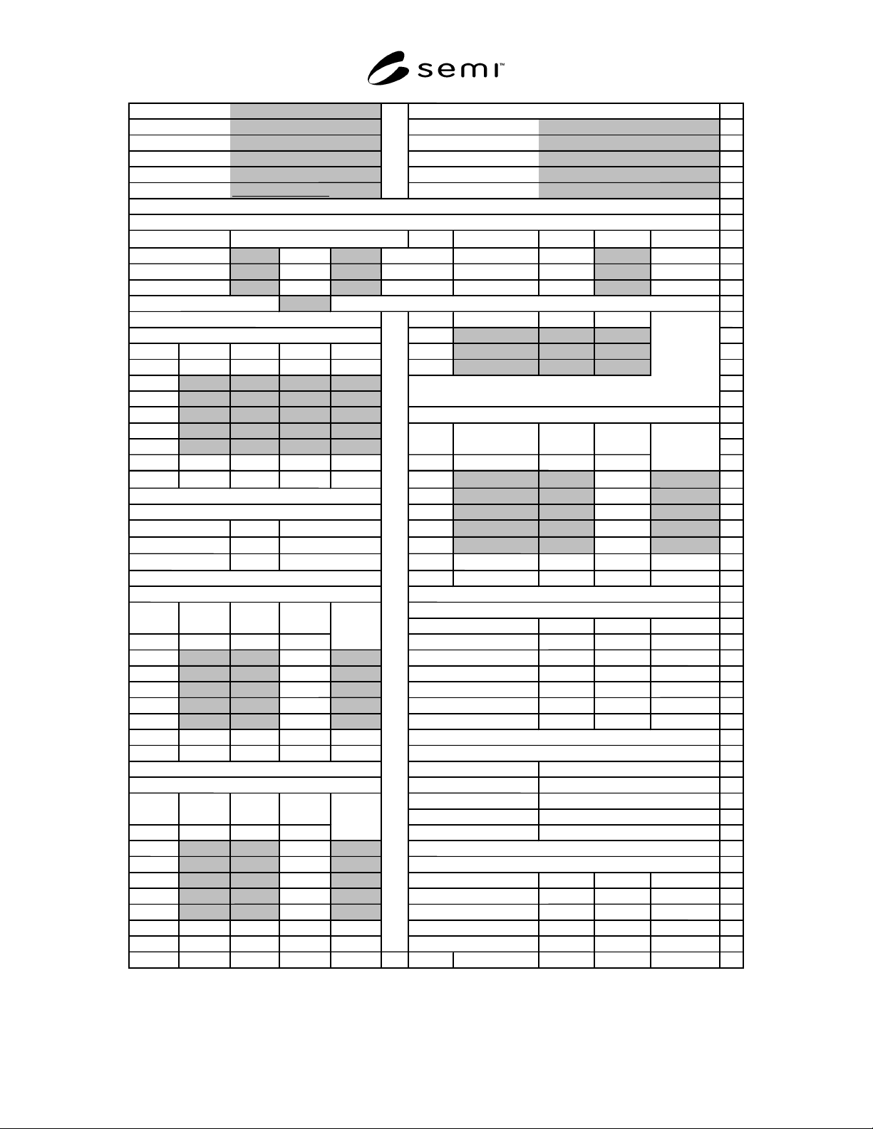
Figure R2-1
Example Test Results

SEMI M58-0704 © SEMI 2004 12
NOTICE: SEMI makes no warranties or representations as to the suitability of the standards set forth
herein for any particular application. The determination of the suitability of the standard is solely the
responsibility of the user. Users are cautioned to refer to manufacturer' s instructions, product labels,
product data sheets, and other relevant literature, respecting any materials or equipment mentioned herein.
These standards are subject to change without notice.
By publication of this standard, Semiconductor Equipment and Materials International (SEMI) takes no
position respecting the validity of any patent rights or copyrights asserted in connection with any items
mentioned in this standard. Users of this standard are expressly advised that determination of any such
patent rights or copyrights, and the risk of infringement of such rights are entirely their own responsibility.
Copyright by SEMI® (Semiconductor Equipment and Materials
International), 3081 Zanker Road, San Jose, CA 95134. Reproduction o
f
the contents in whole or in part is forbidden without express written
consent of SEMI.