semi合集-English.pdf - 第6028页
SEMI G2-94 © SEMI 1 994 8 NOTICE: T hese standards do n ot purport to address safety issues, if any, ass o ciated with their use. It is the responsibility of t he user of these standards to establish appropriate safety a…
SEMI G2-94 © SEMI 19947
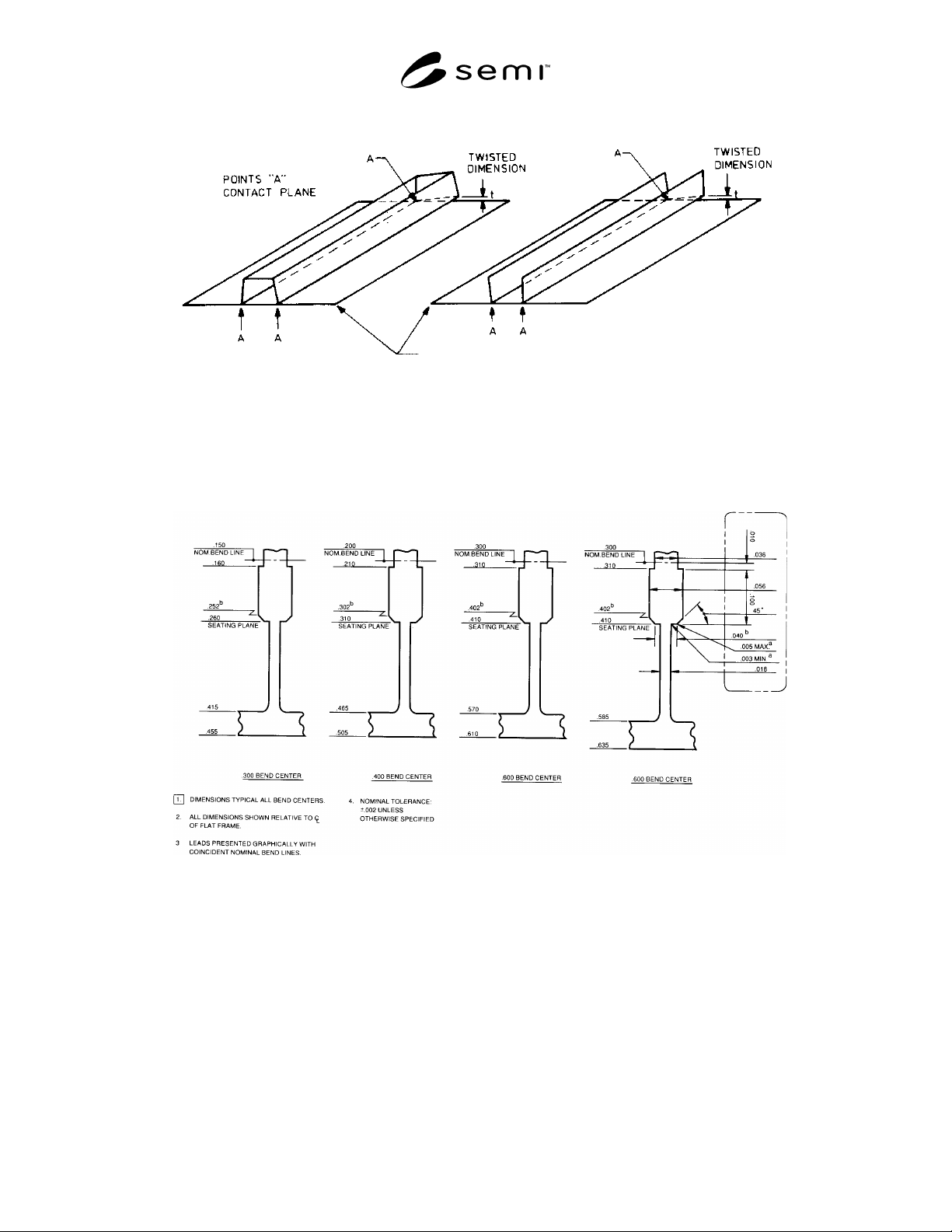
METHOD #1
METHOD #2
REF PLANE
Figure 4
Twist Strip
Using surface plate, establish a reference plane the whole length of the frame strip. Place frame strip, either method
1 or 2, whichever method gives a 3 point contact with reference plane A, using thickness gauges to determine height
between reference plane and 4th point noted as t. This measurement will determine frame twist over entire length.
Figure 5
Standoff Lead Length

SEMI G2-94 © SEMI 1994 8
NOTICE: These standards do not purport to address
safety issues, if any, associated with their use. It is the
responsibility of the user of these standards to establish
appropriate safety and health practices and determine
the applicability of regulatory limitations prior to use.
SEMI makes no warranties or representations as to the
suitability of the standards set forth herein for any
particular application. The determination of the
suitability of the standard is solely the responsibility of
the user. Users are cautioned to refer to manufacturer’s
instructions, product labels, product data sheets, and
other relevant literature respecting any materials
mentioned herein. These standards are subject to
change without notice.
The user’s attention is called to the possibility that
compliance with this standard may require use of
copyrighted material or of an invention covered by
patent rights. By publication of this standard, SEMI
takes no position respecting the validity of any patent
rights or copyrights asserted in connection with any
item mentioned in this standard. Users of this standard
are expressly advised that determination of any such
patent rights or copyrights, and the risk of infringement
of such rights, are entirely their own responsibility.
Copyright by SEMI® (Semiconductor Equipment and Materials
International), 3081 Zanker Road, San Jose, CA 95134. Reproduction o
f
the contents in whole or in part is forbidden without express written
consent of SEMI.
SEMI G3-90 © SEMI 1980, 19961
SEMI G3-90
SPECIFICATION FOR SlDEBRAZED LAMINATES
1 Preface
This specification covers laminated ceramic sidebrazed
packages of 7.62 mm (0.003"), 10.16 mm (0.400"),
15.24 mm (0.600") and 22.86 mm (0.900") nominal
widths. The leadframe which is brazed to this type of
package is included in this specification.
2 Applicable Documents
1
2.1 This following applicable documents, of the
revision currently in effect, are part of this specification
to the extent referenced herein.
MIL-STD-105 — Sampling Procedures and Tables for
Inspection by Attributes
MIL-STD-883 — Test Methods and Procedures for
Microelectronics
MIL-G-45204 — Gold Plating, Electro-Deposited
MIL-M-38510 — General Specification for
Microcircuits
3 Selected Definitions
burr — An adherent fragment of excess parent material
at the component edge.
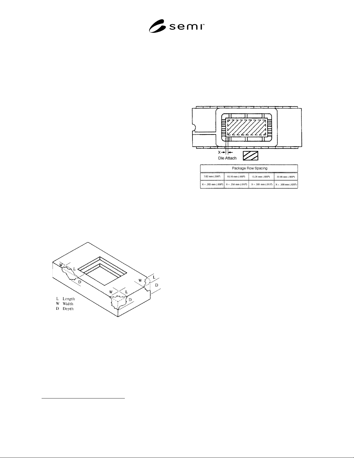
Figure 1
Chip Illustration
chip — A region of ceramic missing from the surface or
edge of a package which does not go completely
through the package. Chip size is given by its length,
width and depth from a projection of the design plan-
form. (See Figure 1.)
1 Military Standards, Naval Publications and Form Center, 5801
Tabor Ave., Philadelphia, PA 19120
crack — A cleavage or fracture that extends to the
surface of a package. It may or may not pass through
the entire thickness of the package.
die attach surface — See Figure 2.
Figure 2
Die Attach Surface
discoloration — Any change in the color of the
package plating as detected by the unaided eye after the
application of heat per Section 9.1.1.
foreign material — An adherent particle other than
parent material of that component.
LSI — Large scale integration.
layer — A ceramic or metallized layer that performs a
discrete function as a part of the package. Should a
layer be comprised of more than one ceramic laminate,
all of those laminates shall be considered as comprising
one layer if all are common in both plan-form and
function. Leadframes shall not be considered as layers.
MSI — Medium scale integration.
projection — An adherent fragment of excess material
on the component surface.
pullback — The linear distance between the edge of the
ceramic and the first measurable metallization interface.
(See Figure 3.)
rundown — See Figure 3.