semi合集-English.pdf - 第5765页
SEMI P20-0703 © SEMI 1992, 2003 4 NOTICE: SEMI makes no warranties or representations as to the suitability o f the standards set forth herein for any particular application. The determination of the suitability o f the …
SEMI P20-0703 © SEMI 1992, 2003 3
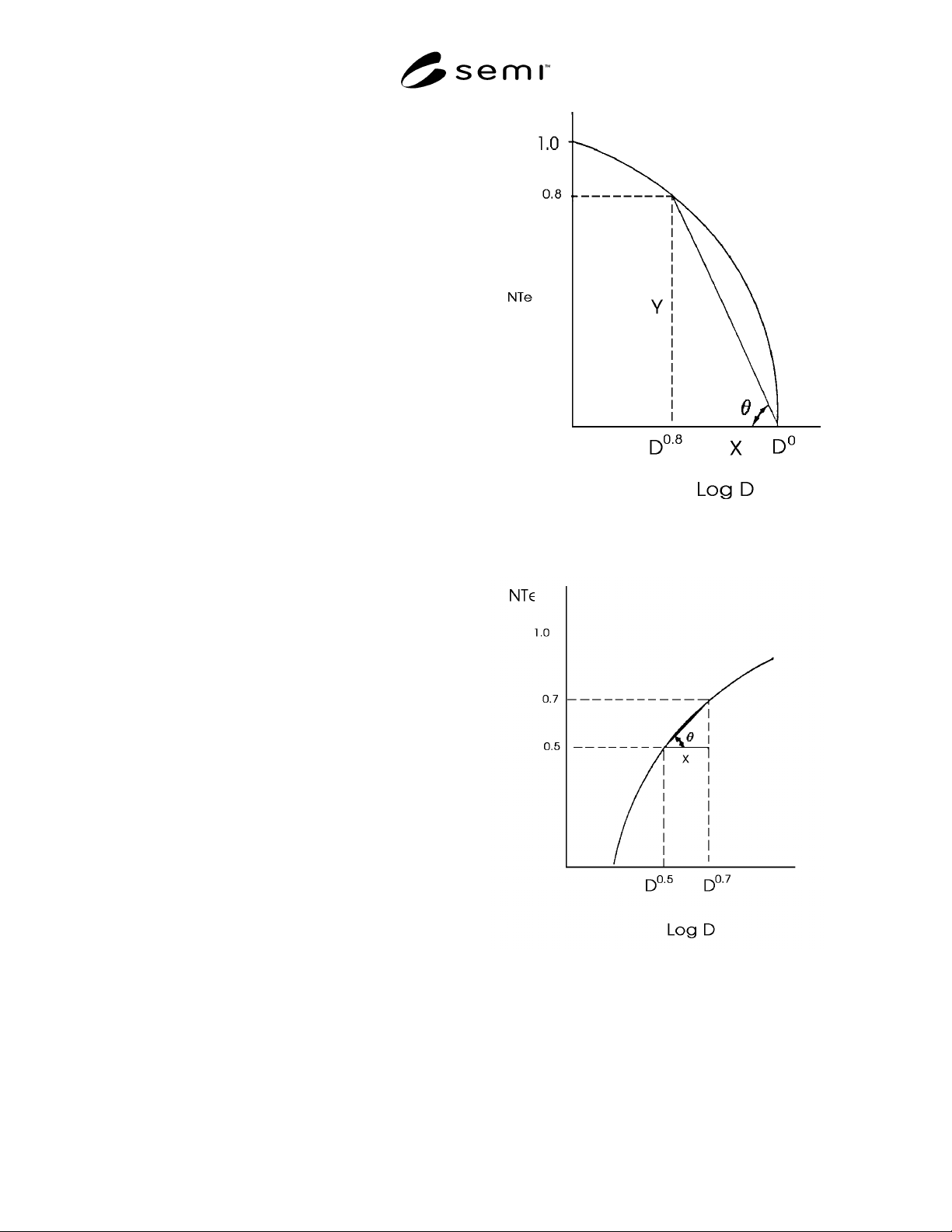
12.3 Negative Resist (Figure 2) — Calculate using an
angle given from a solid line between NTe of 0.5 and
NTe of 0.7 and a solid line parallel to x axis.
γ
p
0.5
−
0.7
= tanθ = y/x = 0.2/log (Dn
0.7
/Dn
0.5
)
13 Resolution
13.1 Pattern Type and Feature Size — Lines and
spaces. Ratio of lines and spaces should be 1:1. Add
hole pattern and isolated pattern if possible.
13.2 Conditions — Specify conditions in Sections 7, 8,
and 9.
13.3 Measurement Method — Measure resolutions
using a scanning electron microscope.
14 Nominal Exposure Dosage
14.1 Nominal Exposure Dosage Definition — A dose
which gives lines and spaces of 3 µm at a ratio of 1:1
under conditions described in Sections 7, 8, and 9.
15 Others
15.1 Describe following items if known.
15.1.1 Durability — Wet etching, dry etching.
15.1.2 Stability — Shelf stability, spun film stability,
post exposure stability, and post processing stability.
15.1.3 Removability — Describe resist removing
method after processing.
15.1.4 Remarks — Describe special characteristics of
the EB resist.
15.1.5 Cautions — Describe cautions for safety.
(Reference) G.N. Taylor, Solid State Technology, June
(1984) 105.
Figure 1
Positive Sensitivity Curve
Figure 2
Negative Sensitivity Curve

SEMI P20-0703 © SEMI 1992, 2003 4
NOTICE: SEMI makes no warranties or
representations as to the suitability of the standards set
forth herein for any particular application. The
determination of the suitability of the standard is solely
the responsibility of the user. Users are cautioned to
refer to manufacturer’s instructions, product labels,
product data sheets, and other relevant literature
respecting any materials mentioned herein. These
standards are subject to change without notice.
The user’s attention is called to the possibility that
compliance with this standard may require use of
copyrighted material or of an invention covered by
patent rights. By publication of this standard, SEMI
takes no position respecting the validity of any patent
rights or copyrights asserted in connection with any
item mentioned in this standard. Users of this standard
are expressly advised that determination of any such
patent rights or copyrights, and the risk of infringement
of such rights, are entirely their own responsibility.
Copyright by SEMI® (Semiconductor Equipment and Materials
International), 3081 Zanker Road, San Jose, CA 95134. Reproduction o
f
the contents in whole or in part is forbidden without express written
consent of SEMI.

SEMI P21-92 © SEMI 1992, 2003 1
SEMI P21-92 (Reapproved 0703)
GUIDELINES FOR PRECISION AND ACCURACY EXPRESSION FOR
MASK WRITING EQUIPMENT
This guideline was technically approved by the Global Micropatterning Committee and is the direct
responsibility of the Japanese Micropatterning Committee. Current edition approved by the Japanese
Regional Standards Committee on April 28, 2003. Initially available at www.semi.org June 2003; to be
published July 2003. Originally published in 1992.
1 Purpose
1.1 This guideline describes general requirements
concerning precision and accuracy expression of mask
writing equipment. Writing accuracy of the mask
writing equipment is evaluated by measuring a written
mask and is affected greatly by process conditions to be
carried out. Therefore, the writing conditions are to be
agreed upon by the user and supplier.
2 Scope
NOTICE: This standard does not purport to address
safety issues, if any, associated with its use. It is the
responsibility of the users of this standard to establish
appropriate safety and health practices and determine
the applicability of regulatory or other limitations prior
to use.
3 Precision and Accuracy Expression Items,
Definitions, Measurement, and Requirements
3.1 Minimum Pattern
3.1.1 Definition
• The minimum line and space pattern and minimum
pattern which is possible to be separated.
3.1.2 Expression
• SEM photograph
3.1.3 Measurement
• SEM photograph of the resist pattern or the chrome
pattern.
3.2 Pattern Dimension Precision and Accuracy
3.2.1 Definition
• Critical Dimension (CD) variation and deviation of
written pattern from designed value.
3.2.2 Expression
• Deviation of measured mean value to design value
(∆l:µm) and variations (3 σ:µm).
• Measured area and number of sampling point
should be clearly described.
3.2.3 Measurement
• Optical CD measurement
• Electron beam CD measurement
• CD measurement done by self-diagnostic feature of
writing equipment.
3.2.4 Requirement
• Width of a long line pattern in X and Y direction
should be measured.
• Pattern types are isolated pattern; 1:1 line and
space pattern or 1:2 line and space pattern.
• The line width to be measured is not specified, but
at least three different line widths should be
measured.
• Examples of patterns are shown in Figures 1 and 2.
3.3 Overlay Accuracy
3.3.1 Definition
• Relative deviation of pattern position between two
masks.
3.3.2 Expression
• 3σ:µm (X and Y direction separately)
• Measured area and number of sampling points
should be clearly described.
3.3.3 Measurement
• Optical coordinates measurement
• Electron beam coordinates measurement
• Coordinates measurement done by self-diagnostic
feature of writing equipment.
3.3.4 Requirement
• The pattern should be cross or L mark. Uniform
rotation error in measurement should be subtracted
from the measurement result.
• Overlay accuracy between different cassette should
be clearly described. An example of a pattern is
shown in Figure 3.