semi合集-English.pdf - 第5971页
SEMI P42-0304 © SEMI 2004 4 Ed g e Cl ear a n ce Sh o t m a p Sh o t Ste p XY S h ot ar ea si ze X, Y WAFER Edge Clearan ce Sho t map Sho t Step XY Shot area si ze X,Y Re t i c l e B a rc ode Reti cl e M a r k Wafer M a …
SEMI P42-0304 © SEMI 2004 3
5.1.38 step pitch — a pitch of matrix arrangement for a
shot. The pitch for the X and Y directions can be
different.
5.1.39 use exposure machine — information related to
equipment used for exposure.
5.1.40 wafer information — information related to the
target wafer for processing.
5.1.41 wafer mark — a mark formed on a wafer for the
purpose of wafer alignment. It can be used to align the
wafer, where reticle image will be projected.
5.1.42 wafer mark position — the mark coordinate
origin as defined by the equipment. It is expressed as
coordinate relative to a reference position of the shot
that exposes a wafer mark or a wafer reference position.
5.1.43 wafer mark type — type of wafer alignment
mark.
5.1.44 wafer rotation — the direction of wafer rotation.
It is defined by exposure tool.
5.1.45 wafer size — the diameter of a wafer.
5.1.46 wafer thickness — thickness of the target wafer
for processing.
5.1.47 wafer type — the identification to use notch or
OF (orientation flat) as a base for the direction of wafer
rotation.
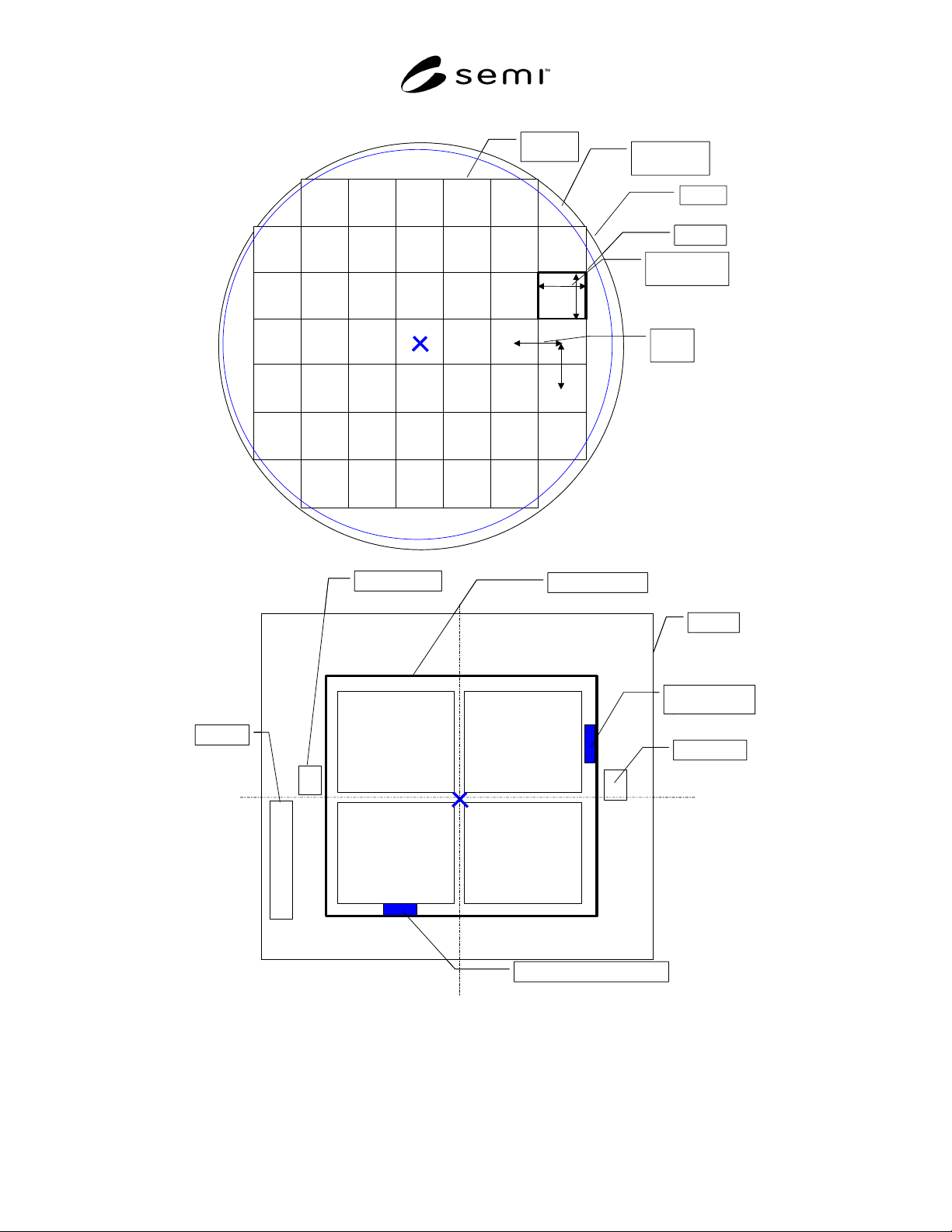
5.2 Figure 2 explains the terminology. Figure 2 is an
example and shall be treated as a supplement data.
6 Reticle Frame Data
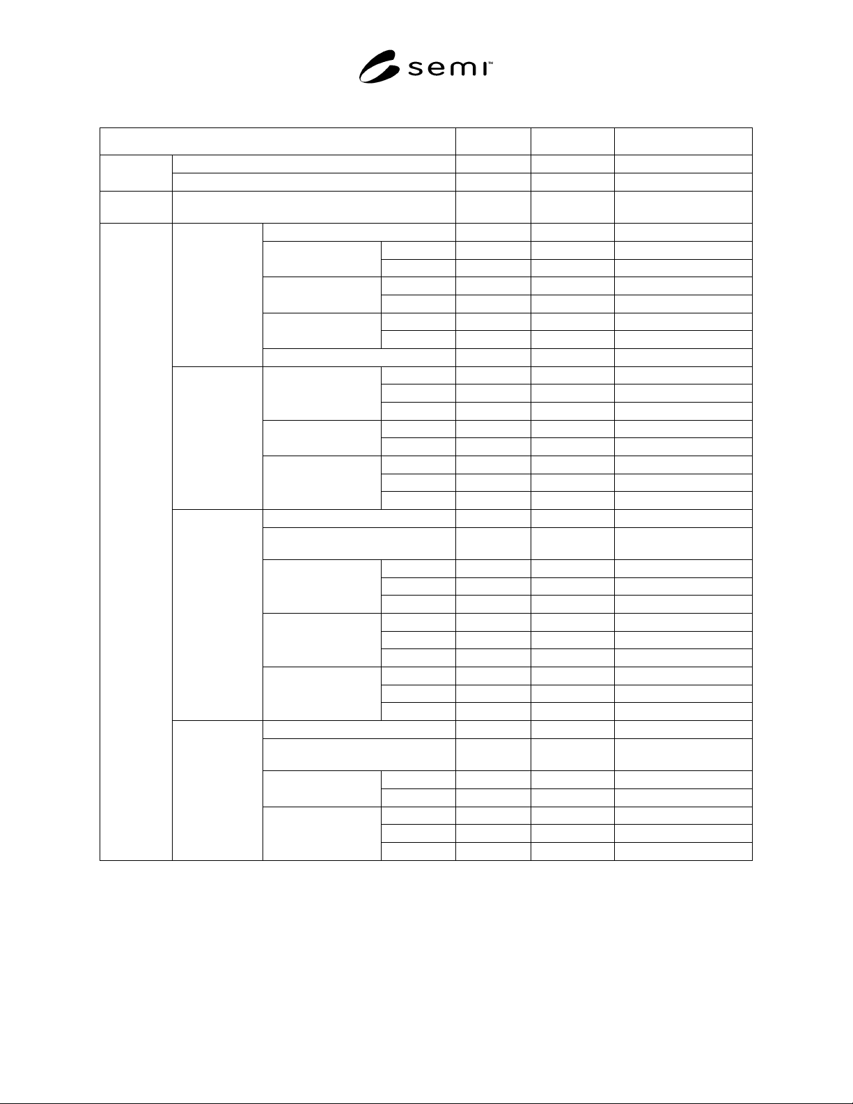
6.1 Reticle frame data is correlated with a hierarchic
configuration as shown in Table 1. The item that
defines the ID in this table can have several pieces of
data. This table is used to generate one recipe of the
exposure equipment. The unit of “µm” in this table is
transcribed as “um”, which can be used as the entry in
XML files.
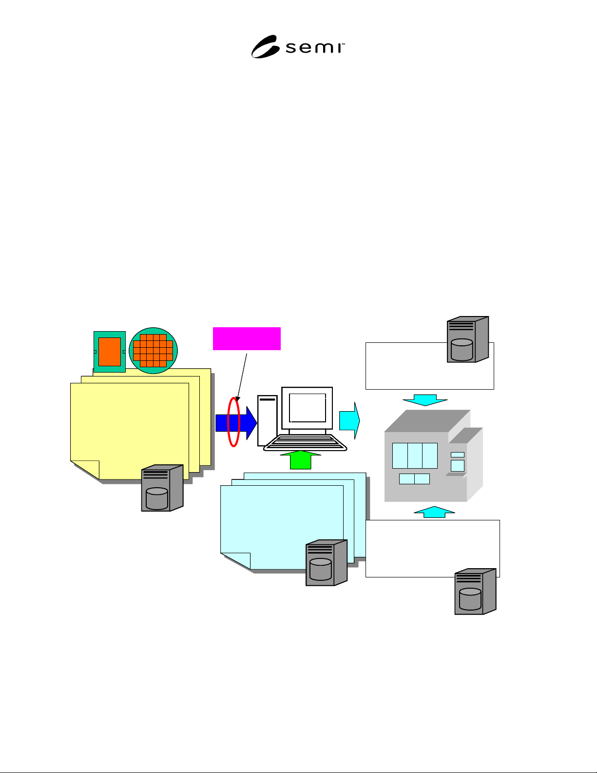
RDM I/F
Design information
Machine type name, process names,
mask name frame design information
1) shot size/shot shifting
2) Alignment mark and coordinate
Wafer map design information
1) shot map
Editing
machine
Process information
(each basis process)
1) Alignment sensor type
2) Alignment shot number/selection shot
3) Focus 4) exposure quantity
5) exposure mode
6)NA, lighting condition
HOST of wafer FAB
(the APC information)
Process revision information
1) exposure quantity revision
2) Alignment revision
Expose tool condition information
1) FOCUS condition 2) stage condition
3) illumination condition
4) Alignment sensor condition
(tool maintenance information)
RDM I/F
Design information
Machine type name, process names,
mask name frame design information
1) shot size/shot shifting
2) Alignment mark and coordinate
Wafer map design information
1) shot map
Editing
machine
Editing
machine
Process information
(each basis process)
1) Alignment sensor type
2) Alignment shot number/selection shot
3) Focus 4) exposure quantity
5) exposure mode
6)NA, lighting condition
HOST of wafer FAB
(the APC information)
Process revision information
1) exposure quantity revision
2) Alignment revision
Expose tool condition information
1) FOCUS condition 2) stage condition
3) illumination condition
4) Alignment sensor condition
(tool maintenance information)
Figure 1
Recipe Preparation of Exposure Machine
SEMI P42-0304 © SEMI 2004 4
Edge
Clearance
Shot map
Shot
Step
XY
Shot area size
X,Y
WAFER
Edge
Clearance
Shot map
Shot
Step
XY
Shot area size
X,Y
Reticle
Barcode
Reticle Mark
Wafer Mark X & positionXY
Wafer Mark Y
positionXY
Shot area size XY
Reticle Mark
Reticle
Barcode
Reticle Mark
Wafer Mark X & positionXY
Wafer Mark Y
positionXY
Shot area size XY
Reticle Mark
Figure 2
Explanation for Terminology
SEMI P42-0304 © SEMI 2004 5
Table 1 Reticle Frame Data
Item Data type Unit the entry example
Date Date Time ---- 1999-05-31T13:20+08:00Formulation
information
Person string ---- HIGASHINO
Use exposure
machine
Machine type information (1 – ∞) string ----
Wafer type string ---- SEMI,JEIDA,OF,notch
Size unsignedInt ---- 150,200,300,5,6,8,12 Wafer size
UnitType string mm/um/inch mm,inch
Clearance Double ---- 3.0 Edge Clearance
UnitType string mm/um/inch mm
Thickness unsignedInt ---- 725 Wafer thickness
UnitType string mm/um/inch um
Wafer
information
Wafer Rotation unsignedInt deg 0,90,180,270,xxx
X Double ---- X size
Y Double ---- Y size
Step Pitch
UnitType string mm/um/inch
C unsignedInt ---- Col Shot Map array
R unsignedInt ---- Row
X Double ---- X offset
Y Double ---- Y offset
Shot Map
information
Shot Map offset
UnitType string mm/um/inch
Shot area ID ID ---- Uniqueness ID
Reticle ID string ---- Reticle information
Reticle ID
X Double ---- X size
Y Double ---- Y size
Shot area size
UnitType string mm/um/inch
X Double ---- X shift
Y Double ---- Y shift
Shot area shift
UnitType string mm/um/inch
X Double ---- X position
Y Double ---- Y position
Shot area
information
(1 – ∞)
Shot area position
shift
UnitType string mm/um/inch
Shot ID ID ---- Uniqueness ID
Shot area ID string ---- Shot area information
Shot area ID
C unsignedInt ---- Column Shot Location
R unsignedInt ---- Row
X Double ---- X position
Y Double ---- Y position
Shot map
Shot information
(1 – ∞)
Shot position
UnitType string mm/um/inch