semi合集-English.pdf - 第6030页
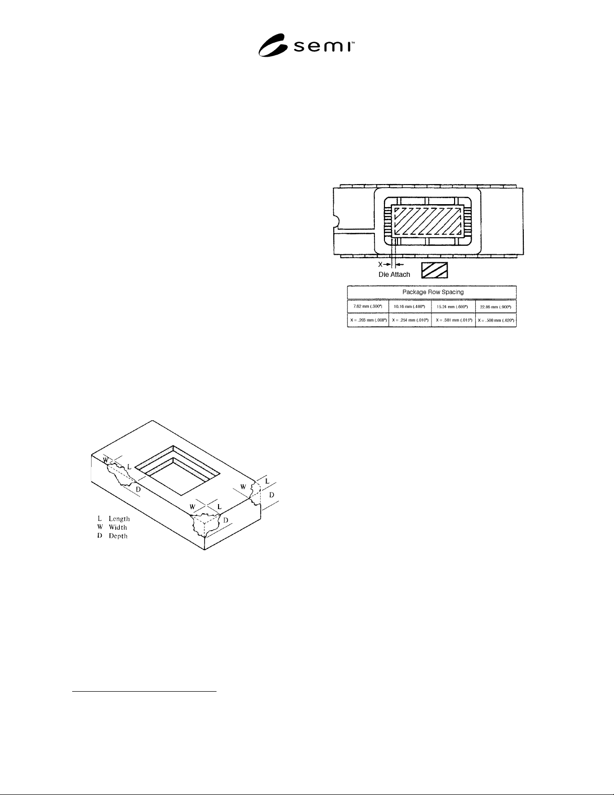
SEMI G3-90 © SEMI 1 980, 199 6 2 Figure 3 Metallizat ion Misa lignment SSI — Small scale integration. seal area — A dimens ional outline area desi gnated f o r either metallization or bare ceramic to pr ovide a surface a…
SEMI G3-90 © SEMI 1980, 19961
SEMI G3-90
SPECIFICATION FOR SlDEBRAZED LAMINATES
1 Preface
This specification covers laminated ceramic sidebrazed
packages of 7.62 mm (0.003"), 10.16 mm (0.400"),
15.24 mm (0.600") and 22.86 mm (0.900") nominal
widths. The leadframe which is brazed to this type of
package is included in this specification.
2 Applicable Documents
1
2.1 This following applicable documents, of the
revision currently in effect, are part of this specification
to the extent referenced herein.
MIL-STD-105 — Sampling Procedures and Tables for
Inspection by Attributes
MIL-STD-883 — Test Methods and Procedures for
Microelectronics
MIL-G-45204 — Gold Plating, Electro-Deposited
MIL-M-38510 — General Specification for
Microcircuits
3 Selected Definitions
burr — An adherent fragment of excess parent material
at the component edge.
Figure 1
Chip Illustration
chip — A region of ceramic missing from the surface or
edge of a package which does not go completely
through the package. Chip size is given by its length,
width and depth from a projection of the design plan-
form. (See Figure 1.)
1 Military Standards, Naval Publications and Form Center, 5801
Tabor Ave., Philadelphia, PA 19120
crack — A cleavage or fracture that extends to the
surface of a package. It may or may not pass through
the entire thickness of the package.
die attach surface — See Figure 2.
Figure 2
Die Attach Surface
discoloration — Any change in the color of the
package plating as detected by the unaided eye after the
application of heat per Section 9.1.1.
foreign material — An adherent particle other than
parent material of that component.
LSI — Large scale integration.
layer — A ceramic or metallized layer that performs a
discrete function as a part of the package. Should a
layer be comprised of more than one ceramic laminate,
all of those laminates shall be considered as comprising
one layer if all are common in both plan-form and
function. Leadframes shall not be considered as layers.
MSI — Medium scale integration.
projection — An adherent fragment of excess material
on the component surface.
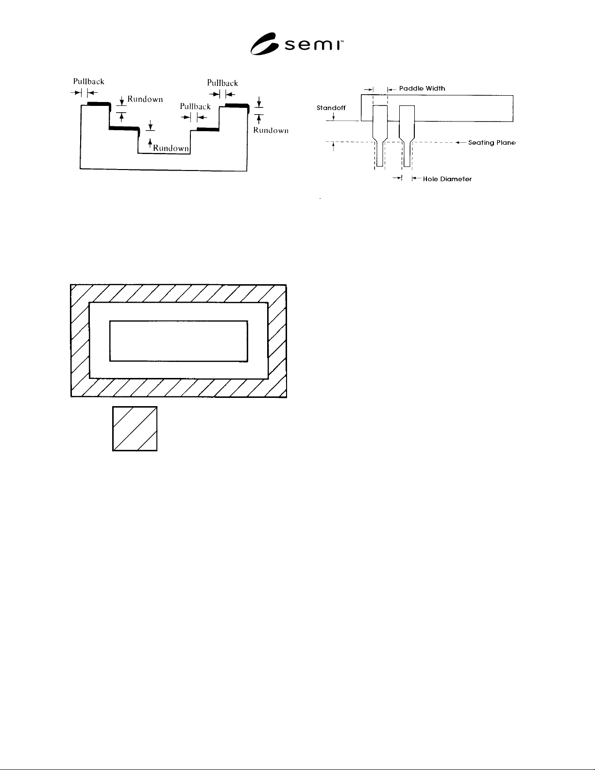
pullback — The linear distance between the edge of the
ceramic and the first measurable metallization interface.
(See Figure 3.)
rundown — See Figure 3.
SEMI G3-90 © SEMI 1980, 1996 2
Figure 3
Metallization Misalignment
SSI — Small scale integration.
seal area — A dimensional outline area designated for
either metallization or bare ceramic to provide a surface
area for sealing. (See Figure 4.)
Figure 4
Seal Area
seating plane — See Figure 5.
standoff — Residual air gap after inserting the leads
into a ground steel plate with a specific size hole and
applying a specified downward pressure. (See Figure
5.)
NOTE: When determining the seating plane a downward
f
of 10 grams is to be applied to the package.
Figure 5
Leadframe Paddle Width and Standoff
TIR — Total indicator reading.
VLSI — Very large scale integration.
void — An absence of metallization or plating from a
designated area.
4 Ordering Information
Purchase orders for sidebrazed laminated packages
furnished to this specification shall include the
following items:
1. Drawing number and revision level
2. Number of leads and lead series spacing
3. Type and color of ceramic
4. Type and thickness of plating
5. Description (See Table 1.)
6. Thickness of individual layers of ceramic
7. Internal finger bonding pattern layout
8. Minimum exposed metallized bond finger length
and width
9. Leads common to die attach area and/or seal ring
10. Sealing dimensions and flatness
11. Certification
12. Method of test and measurements (See Section 9.)
13. Lot acceptance procedures (See Section 8.)
14. Packaging and Marking (See Section 10.)
5 Dimensions and Permissi ble Variations
The dimensions of the sidebraze laminate packages
shall conform as specified in Table 1.

SEMI G3-90 © SEMI 1980, 19963
6 Materials
6.1 Ceramic
6.1.1 Alumina content 90% minimum.
6.1.2 Color — Opaque or white.
6.2 Metallization
6.2.1 Refractory metallization (provide adequate bond
strength to ceramic).
6.2.2 Nickel plating (if designated).
6.2.3 Precious or noble metal plating.
6.2.4 Nickel/gold per MIL-M-38510 except gold
plating shall conform to MIL-G-45204, Type III and
have a thickness of 60 microinches minimum.
6.3 Braze Material — An alloy with a melting point
equal to or greater than 750°C which will provide
specified bond strength of the lead to the ceramic.
6.4 Lead Material
6.4.1 Iron nickel cobalt alloy per MIL-M-38510, Type
A.
6.4.2 Iron nickel alloy per MIL-M-38510, Type B.
7 Defect Limits
7.1 Ceramic
7.1.1 Cracks — None allowed.
7.1.2 Chips
7.1.2.1 Corner — 0.762 mm (0.030") × 0.762 mm
(0.030") × 0.762 mm (0.030") max.
7.1.2.2 Edge — 2.54 mm (0.100") × 0.762 mm
(0.030") × 0.762 mm (0.030") max. (Chips can not be
encroached or exposed any metallized area.)
7.1.2.3 Seal Area
7.1.2.3.1 7.62 mm (0.300") and 10.16 mm (0.400")
Row Spacing Parts — .762 mm (0.030") × 2.54 mm
(0.100")
7.1.2.3.2 15.24 mm (0.600") Row Spacing Parts —
1.27 mm (0.050") × 0.381 mm (0.015") × 0.381 mm
(0.015") max.
7.1.2.3.3 22.86 mm (0.900") Rowing Spacing Parts —
1.52 mm (0.060") × 0.508 mm (0.020") × 0.508 mm
(0.020") max.
7.1.2.3.4 Chips cannot reduce the seal width by more
than 1/3 of the design width.
7.1.3 Burrs and Projections
7.1.3.1 Top Plane Excluding Seal Area — 0.102 mm
(0.004") max.
7.1.3.2 Seal Area — 0.025 mm (0.001") max. above
metallization.
7.1.3.3 Wire Bond Finger Areas — 0.025 mm (0.001")
max. above metallization.
7.1.3.4 Die Attach Surface — 0.025 mm (0.001") max.
above metallization excluding a 0.203 mm (0.008")
perimeter on 7.62 mm (0.300") centerline packages,
0.254 mm (0.010") perimeter on 10.16 mm (0.400")
centerline packages and 0.381 mm (0.015") perimeter
on 15.24 mm (0.600") centerline packages, 0.508 mm
(0.020") perimeter on 22.86 mm (0.900") row center
package.
7.1.4 Camber — Ceramic-maximum of 0.004
inch/inch (mm/mm).
7.1.5 Flatness
7.1.5.1 Seal Area — 0.050 mm (0.002") TIR on 7.62
mm (0.300") row center packages, 0.0635 mm
(0.0025") TIR on 10.16 mm (0.400") and 15.24 mm
(0.600") row center packages.
7.1.5.2 Die Attach — Die attach pad to be flat to
within 0.051 mm (0.002") TIR to exclude a 0.203 mm
(0.008") perimeter on 7.62 mm (0.300") centerline
packages, 0.254 mm (0.010") perimeter on 10.16 mm
(0.400") centerline packages and 0.381 mm (0.015")
perimeter on 15.24 mm (0.600") centerline packages.
7.2 Metallization
7.2.1 Voids
7.2.1.1 Seal Area — On the outer half of the seal area
width, maximum of 3 voids no larger than 0.127 mm
(0.005") in diameter are permissible. On the inner half,
maximum of 3 voids no larger than 0.381 mm (0.015")
in diameter or larger than 1/3 of the seal area width,
whichever is the smaller. The distance between any 2
voids shall be at least 0.762 mm (0.030").
7.2.1.2 Wire Bond Fingers — A 0.254 mm (0.010") ×
0.010" (0.254 mm) void free area within the specified
wire bond finger area as defined be the procurement
drawing.
7.2.1.3 Die Attach Surface — Maximum 0.010"
(0.254 mm) diameter by a distance greater than 0.030"
(0.762 mm) with no more than 3 voids.
7.2.2 Metallization Misalignment — See Figure 3.
7.2.2.1 Seal Plane Rundown — Internal cavity — not
to exceed 25% of the cavity layer thickness. External
cavity — not to be less than 0.010" (0.254 mm) outside
the cavity.