semi合集-English.pdf - 第4920页
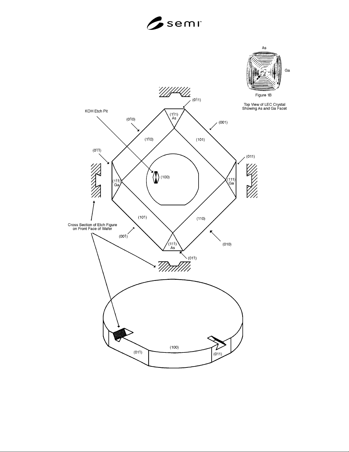
SEMI M9-0999 © SEMI 1986, 1999 5 Figures 1A an d 1B Both Diagram s Show a GaAs Wafer with Su rface Orientation A and Flat Option V-Groove
SEMI M9-0999 © SEMI 1986, 1999 4
shall be certified as “capable of meeting” certain
requirements. In this context, “capable of meeting”
shall signify that the supplier is not required to perform
the appropriate tests in Section 9. However, if the
purchaser performs the test and the material fails to
meet the requirement, the material may be subject to
rejection.
12 Packing and Marking
12.1 Special packing and marking requirements shall
be subject to agreement between the supplier and the
purchaser. Otherwise, all wafers shall be handled,
inspected, and packed in such a manner as to avoid
chipping, scratches, and contamination in accordance
with the best industry practices to provide ample
protection against damage during shipment.
12.2 The wafers supplied under these specifications
shall be identified by appropriately labeling the outside
of each box or other container and each subdivision
thereof in which it may reasonably be expected that the
wafers will be stored prior to further processing.
Identification shall include as a minimum the nominal
diameter, conductive dopant, orientation, resistivity
range, and lot number.
12.3 The lot number, either (1) assigned by the
original manufacturer of the wafers, or (2) assigned
subsequent to slice manufacture but providing reference
to the original lot number, shall provide easy access to
information concerning the fabrication history of the
particular wafers in that lot. Such information shall be
retained on file at the manufacturer’s facility for at least
one month or as negotiated between vendor and user
after that particular lot has been accepted by the
purchaser.
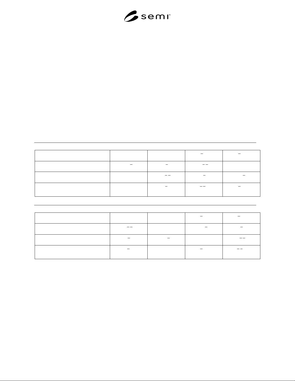
Table 1. Equivalent Orientations
V-Groove Option
Surface orientation:
)100()100(
)001( )001(
Primary flat location:
)101( )110( )110(
)011(
Secondary flat location:
)011(
)110(
)110(
)101(
For Surface orientation B, the off-
orientation tilt direction is toward:
)110(
)011( )011( )101(
Table 2. Equivalent Orientations
Dove-Tail Option
Surface orientation:
)100()100(
)001( )001(
Primary flat location:
)110(
)011(
)101(
)110(
Secondary flat location:
)110(
)101(
)011(
)110(
For Surface orientation B, the off-
orientation tilt direction is toward:
)011(
)110(
)101( )011(
The symmetry of GaAs crystal structure allows other Miller indices to be used for identifying surface and flat orientations. This
table lists various possibilities which meet the requirements for the above two options.
NOTE: For V-Groove Option, the relative directions in a single column must be maintained. For Dove-Tail Option, any of the
110 tilt directions are considered equivalent.
SEMI M9-0999 © SEMI 1986, 19995
Figures 1A and 1B
Both Diagrams Show a GaAs Wafer with Surface Orientation A and Flat Option V-Groove
SEMI M9-0999 © SEMI 1986, 1999 6
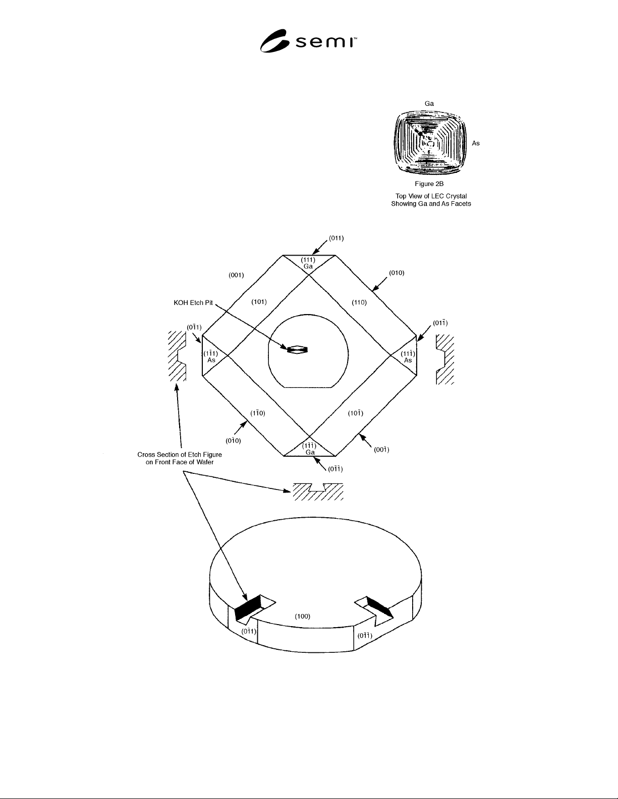
Figures 2A and 2B
Both Diagrams Show a GaAs Wafer with Surface Orientation A and Flat Option Dove-Tail