semi合集-English.pdf - 第6126页
SEMI G27-89 © SEMI 198 5, 1989 3 6.4.1 The lead spacin g and lead loca t i o n that can be maintained is a function of th e designed lead spacing and lead wid th. Desi gn Lead Widt h Desi gn Lead Space Minimu m Lead Sapc…
SEMI G27-89 © SEMI 1985, 1989 2
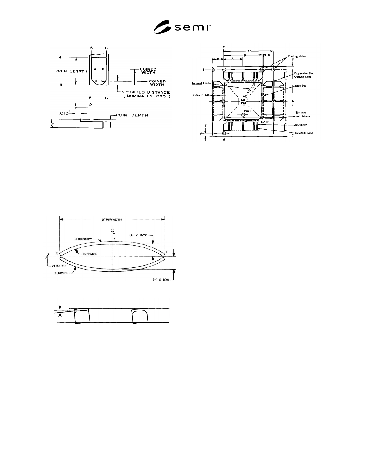
Figure 3
Coined Area
crossbow — transverse bowing of the leadframe (see
Figure 4).
functional area — the die attach pad and the lead tips.
lead twist — angular rotation of bonding fingers (see
Figure 5).
pits — shallow surface depression or craters in the
leadframe material.
Figure 4
Crossbow
Figure 5
Lead Twist
slug marks — random dents in the leadframe caused by
foreign material in the stamping die.
stamped leadframe terminology — (See Figure 6.)
true position circle — the circle with its center
positioned at the center of the coined lead which
defines the design position of the lead tip.
Figure 6
Plastic Leaded Chip Carrier Leadframe
4 Ordering Information
4.1 Purchase orders for leadframes furnished to this
specification shall include the following information:
4.1.1 Current revision of the leadfra me drawing
detailing the base material and the plating type(s),
thickness(es) and area(s).
4.1.2 Reference to this specification.
4.1.3 Vendor certification requirements.
5 Dimensions
See Table 1.
6 Defect Limits and Parame ters
Note: Measurement methods are described in SEMI G10.
Alternate methods may be used as agreed to between vendor
and customer. The methods described in SEMI G10 are
considered to be standard for the purpose of solving
differences.
6.1 Dimensional Tolerances — Se e Figure 6.
6.2 Minimum Flat Wire Bonding Area — 80% of
nominal lead width and 0.635 mm (0.025") in length.
6.3 Coined Depth — 0.013 mm (0 .0005") min. to 30%
of material thickness maximum.
6.4 Horizontal Lead Spacing and Location (Lead
Tips)
SEMI G27-89 © SEMI 1985, 19893
6.4.1 The lead spacing and lead loca tion that can be maintained is a function of the designed lead spacing and lead
width.
Design Lead
Width
Design Lead
Space
Minimum
Lead Sapce
Minimum True
Position Circle Dia.
≥ 0.011" ≥ 0.011" 0.006" 0.007"
0.010" 0.010" 0.005" 0.006"
Tolerances for lead designs smaller than .010" should be negotiated between vendor and user.
6.4.2 18 - 100 Pin Lead Frames — Leads to be located so that a 0.007" diameter circle centered on the nominal
center of the coined lead in width and 0.152 mm (0.006") back from lead tip in length shall be totally encompassed
by the coined area.
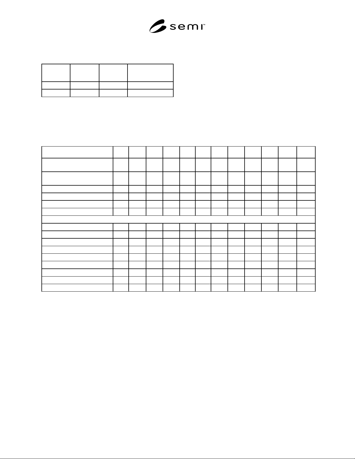
Table 1 Plastic Leaded Chip Carrier Leadframe Standard Dimensions (all dimensions in inches)
LEAD COUNT 18 LD 18 LD 20 LD 28 LD 28 LD 32 LD 44 LD 52 LD 68 LD 84 LD 100 LD 100 LD
PACKAGE SHAPE
Rect.
Rect.
Stretch Square Square Rect. Rect. Square Square Square Square Square Square
JEDEC
PACKAGEDESIGNATION
AA AB AA AB AD AE AC AD AE AF
Nominal Pkg. Width 0.290 0.290 0.350 0.450 0.350 0.450 0.650 0.750 0.950 1.150 1.350 1.150
Length 0.425 0.490 0.350 0.450 0.550 0.550 0.650 0.750 0.950 1.150 1.350 1.150
PROGRESSION 0.720 0.720 0.780 0.880 0.780 0.880 1.080 1.180 1.400 1.600 1.800 1.600
STRIP WIDTH 0.970 1.230 0.970 1.070 1.230 1.230 1.230 1.430 1.670 1.870 2.070 1.870
TOOLING DIMENSIONS (See Figure 6)
A 0.170 0.170 0.200 0.250 0.200 0.250 0.350 0.400 0.500 0.600 0.700 0.600
B 0.340 0.340 0.400 0.500 0.400 0.500 0.700 0.800 1.000 1.200 1.400 1.200
C 0.530 0.530 0.590 0.690 0.590 0.690 0.890 0.990 1.200 1.400 1.600 1.400
D 0.190 0.190 0.190 0.190 0.190 0.190 0.190 0.190 0.200 0.200 0.200 0.200
E 0.020 0.020 0.020 0.020 0.020 0.020 0.020 9.020 0.020 0.020 0.020 0.020
F 0.050 0.050 0.050 0.050 0.050 0.050 0.050 0.050 0.050 0.050 0.050 0.050
G 0.920 1.180 0.920 1.020 1.180 1.180 1.180 1.380 1.620 1.820 2.020 1.820
Diameter 0.060 0.060 0.060 0.060 0.060 0.060 0.060 0.060 0.060 0.060 0.060 0.060
Metal Thickness 0.010 0.010 0.010 0.010 0.010 0.010 0.010 0.010 0.008 0.008 0.008 0.008
Note 1: Gate — All packages; gate on the corner counter-clockwise from pin one.
Note 2: Dam Bar — Recommend 0.025 wide with 0.025 space between package and dam bar.
Note 3: Lead shall meet the JEDEC Quad Package requirements.
6.5 Horizontal Die Attach Pad Lo cation — Die attach pad shall be located within 0.051 mm (± 0.002") on 18-100
pin leads.
6.6 Lead Twist — Shall not exceed 3° 30' or 0.015 mm (0.0006") per 0.254 mm (0.010") of lead width.
6.7 Die Attach Pad Tilt and Flatness
6.7.1 Tilt — 0.025 mm (0.001") maximum per 2.54 mm (0.100") of length or width in the undepressed state. 0.051
mm (0.002") maximum per 2.54 mm (0.100") of length or width in the depressed conditions when measuring from
corner to corner.
6.7.2 Flatness — 0.005 mm (0.0002") per 0.100" pad length on 18-100 pin leadframes when measuring from the
center to the average of the four corners. The corners are defined at 0.127 mm (0.005") from each edge.
6.8 Die Attach Pad Downset or De pression — The nominal downset recommended is 0.015" (0.381 mm) ± 0.002".
6.9 Lead and Die Attach Pad Cop lanarity
SEMI G27-89 © SEMI 1985, 1989 4
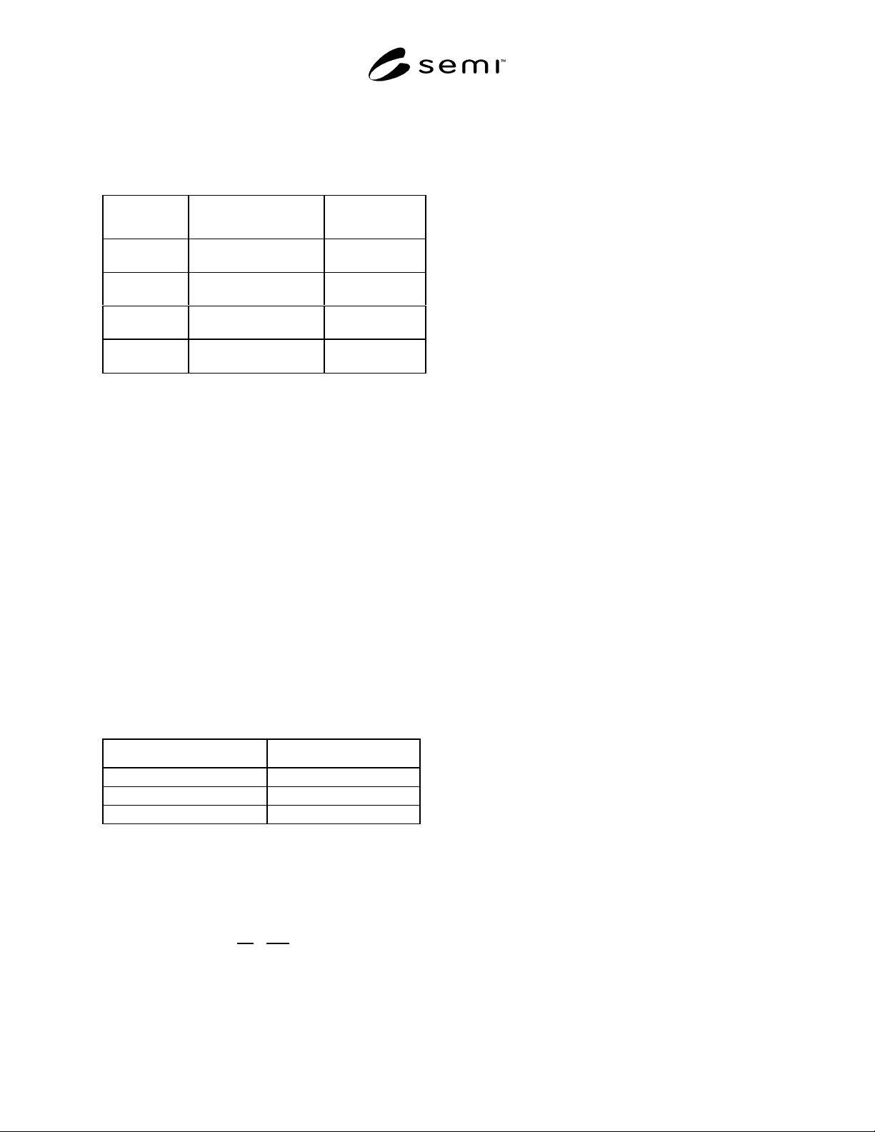
6.9.1 Lead Planarity — The lead tips shall be within
the following tolerances of the Z plane in the taped or
untaped condition.
Table 2 Taped or Untaped Condition
No. of Leads Strip Width
Lead Tip
Coplanarity
18 Rect. 1.070" - 1.230"
(27.18 mm - 31.24 mm)
± 0.003"
(0.76 mm)
20 Square 0.970"
(24.64 mm)
± 0.003"
(0.076 mm)
28-52 1.070" - 1.470"
(27.18 mm - 37.34 mm)
± 0.004"
(0.120 mm)
64-84 1.670" - 1.870"
(42.42 mm - 47.50 mm)
± 0.005"
(0.127 mm)
6.9.2 Die Attach Pad Planarity — T he die attach pad
shall be within the following tolerances of the Z plane.
6.10 Material
6.10.1 0.203 mm (0.008") material thickness
recommended for greater than 52 leads.
6.10.2 0.254 mm (0.010") material thickness
recommended for 52 lead and below.
6.10.3 Nominal thickness tolerances for both Alloy 42
and copper materials of 0.203 mm (0.008") and 0.254
mm (0.010") shall be 0.008 mm (± 0.0003").
6.10.4 Width Tolerance — 0.051 mm (± 0.002") for
both Alloy 42 and copper.
6.11 Coil Set — Maximum of 0.508 mm (0.020") over
the nominal strip length. Does not include material
thickness.
6.12 Crossbow — Crossbow shall not exceed the
following dimensions:
No. of Leads Maximum Crossbow
18—20 ± 0.005" (0.127 mm)
28 - 52 ± 0.006" (0.152 mm)
68 - 84 ± 0.010" (0.254 mm)
6.13 Camber — Shall not exceed 0 .002" over nominal
strip lengths of 8 ± 2 inches.
The relationship to determine maximum camber for
other lengths is approximated as follows:
C
1
C
2
=
L
1
2
L
2
2
6.14 Progression — The progression over the nominal
strip length shall be within 0.051 mm (± 0.002") and
noncumulative.
6.15 Burrs — Shall be firmly attach ed and able to
withstand a probe force of 10 grams. Vertical burrs
inside the dambar shall not exceed 0.025 mm (0.001").
Vertical burrs outside the dambar and horizontal burrs
in any location shall not exceed 0.051 mm (0.002").
6.16 Pits and Slugmarks
6.16.1 Within functional area and on external leads,
there shall be no slugmarks. Pits shall not exceed 0.008
mm (0.0003") in depth and 0.013 mm (0.0005") in
largest surface dimension in these areas.
APPLICATION NOTE: There is a question regarding the
ability of material suppliers to meet this specification.
Revision of this specification is under review.
6.16.2 In other areas, pits and imperfections shall not
affect leadframe strength regardless of size and shall
not exceed 0.051 mm (0.002") in depth and 0.127 mm
(0.005") in largest surface dimension.
6.17 Strip Cut Off Location — Strip cut off shall be
within 0.076 mm (± 0.003") of basic strip length (see
Figure 6).
6.18 Coining and Metal Clearance
6.18.1 Dimensions shown on drawing s are before coin
dimensions.
6.18.2 Maximum coining bulge shall not exceed 0.051
mm (0.002") per edge and shall be governed by metal
to metal clearance requirements (lead to lead and lead
to pad).
6.18.3 Metal to Metal Clearance — Shall be as agreed
to between vendor and customer.
7 Sampling
7.1 The sampling plan shall be agr eed upon between
vendor and customer.
8 Packaging and Marking
8.1 Packaging — Containers and packaging materials
shall be selected to provide protection against normal
transportation damage risks and spillage. They will also
offer protection from contamination, exposure to
moisture, oxidation, and tarnishing.