semi合集-English.pdf - 第6485页
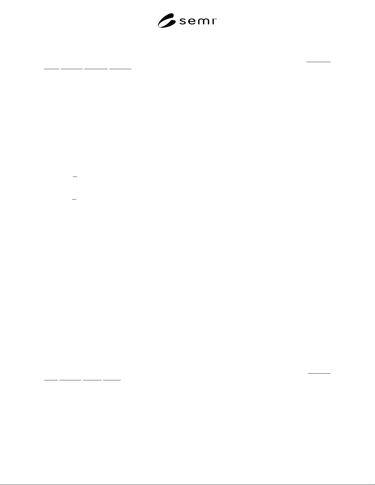
SEMI G78-0699 © SE MI 1999 18 A1-1 .1 5 Step 13 — Calcu late Normaliz e d (b y lot) Die Offset (11) = Average D ie Offset (3) - Av erage Lot Offset (9) [Accu racy] loti setj w afk diel loti setj wafk diel loti setj wafk …
SEMI G78-0699 © SEMI 199917
A1-1.11 Step 9 — Calculate
W-W-X or W-W-Y = 3σ of Normalized (by setup) Wafer Offset (8).
A1-1.11.1 A 3σ variation will be calculat ed based on the normalized wafer offset and will be cited as the Wafer-to-
Wafer variation (W-W-X, W-W-Y).
A1-1.11.2 Discusssion of W-W-X or W-W -Y (Wafer-to-Wafer variation in the X-direction, Wafer-to-Wafer
variation in the Y-direction)
A1-1.11.2.1 This equation will produce a v alue for the 3σ variation from Wafer-to-Wafer in the X and Y
directions. If this number were large, it would tend to indicate that the prober does not behave repeatably from
wafer-to-wafer. Possible causes are:
• loading problems
• temperature stability issues, and
• wafer rotation issues
A1-1.12 Step 10 — Calculate
Average Lot Offset (9) = average of Average Setup Offset (7).
LOTX xoff
LOTY yoff
loti setj
j
loti setj
j
=
=
=
=
1
3
1
3
1
3
1
3
,
,
(9)
A1-1.12.1 Discussion of Average Lot Offset (LOTX or LOTY)
A1-1.12.1.1 This will be one of the values added to the graph. This is simply the average of all of the average die
offsets in the X-direction and all of the average die offsets in the Y-direction. If one needed to pick a single number
in X and Y to describe the accuracy of the prober – this is the one. This can be very misleading though – what this
number really tells you is what value the distribution is centered around. Refer to the graph to get a visual sense of
this data.
A1-1.13
Step 11 — Calculate
Normaliz ed (by lot) Setup Offset (10) = Average Setup Offset (7) - Average Lot
Offset (9)
loti setj
loti setj
loti setj loti setj
xnorm
xoff
ynorm yoff
LOTX
LOTY
,
,
,,
=−
=−
(10)
A1-1.13.1 Discussion of Normalized (by lot) Setup Offset
A1-1.13.1.1 This is another normalization step used to calculate the true setup-to-setup error in X and Y.
A1-1.14 Step 12 — Calculate
S-S-X or S-S-Y = 3σ of Normalized (by lot) Setup Offset (10).
A1-1.14.1 A 3σ variation will be calculat ed based on the normalized setup offset and will be cited as the Setup-to-
Setup variation (S-S-X, S-S-Y).
A1-1.14.2 Discussion of S-S-X or S-S-Y (Setup-to-Setup variability in the X-direction, Setup-to-Setup variability in
the Y-direction)
A1-1.14.2.1 These two values describe how much variability there is between setups.
SEMI G78-0699 © SEMI 1999 18
A1-1.15 Step 13 — Calculate
Normaliz ed (by lot) Die Offset (11) = Average Die Offset (3) - Average Lot Offset
(9) [Accuracy]
loti setj wafk diel
loti setj wafk diel
loti setj wafk diel loti setj wafk diel
xn
xoff
yn yoff
LOTX
LOTY
,, ,
,, ,
,, , ,, ,
=−
=−
(11)
A1-1.15.1 Discussion of Normalized (by lot) Die Offset
A1-1.15.1.1 This step is useful if you need to compare the variation between several different lots. It is not
completely necessary for the next step, since subtracting a constant from a string of numbers does not change the 3σ
variation, only the center point.
A1-1.16 Step 14 — Calculate
TTLX or TTLY = 3σ of Normalized (by lot) Die Offset (11) [Repeatability]
A1-1.16.1 Discussion fo TTLX or TTLY
A1-1.16.1.1 This is the value for determini ng (with 3σ confidence) whether your probe marks will always fall
within your desired spec. They are the hatch-marked lines.
A1-1.17 Step 15 — This normalized die offset includes Die-to-Die, Wafer-to-Wafer, and Setup-to-Setup offsets
thus a 3σ variation of this offset will be called Total Prober
Variation (TTLX and TTLY).
A1-1.17.1 Calculate Total Prober Error Range (3
σ
).
LOTX + TTLX, LOTX - TTLX = Total Prober X-Error Range (3σ)
LOTY + TTLY, LOTY - TTLY = Total Prober Y-Error Range (3σ)
A1-1.17.2 Suggested Graphs:
X-Offset Y-Offset
LOTX + TTLX LOTY + TTLY
LOTX LOTY
LOTX - TTLX LOTY - TTLY
Average Die X-Offset (3) Average Die Y-Offset (3)
A1-1.17.2.1
It is recommended to create on e graph illustrating the prober accuracy in X and one graph for Y.
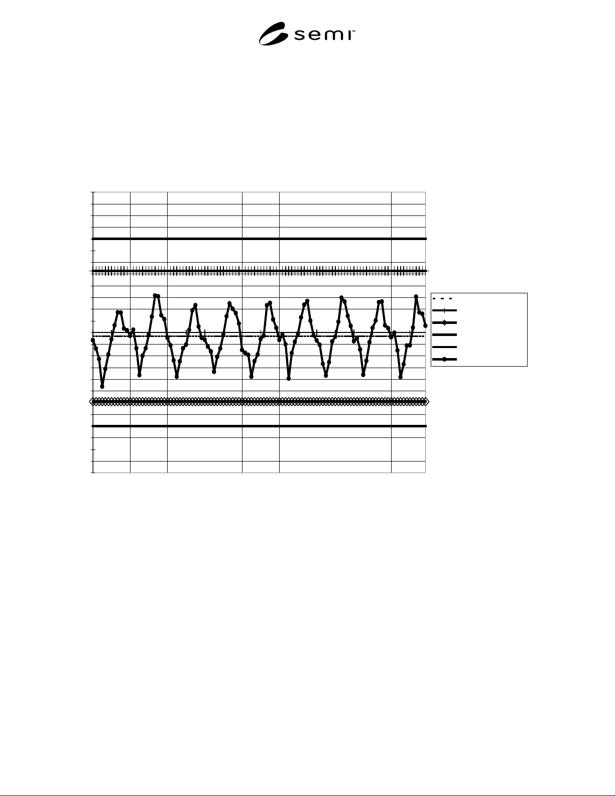
A1-1.18 Discussion of Graphs (one exa mple for X [Figure X] and one for Y [Figure Y])
A1-1.18.1 Average Lot X-Offset is the va lue from Step 10. This number shows where the probe mark distribution
is centered (the accuracy of the prober).
A1-1.18.2 Average Lot X-Offset +3σ is t he result from step 10 + the result from step 14
A1-1.18.3 Average Lot X-Offset -3σ is th e result from step 10 – the result from step 14
A1-1.18.4 These two lines show the ± 3σ range of your distribution. This describes the repeatability of the prober.
NOTE: There will always be explainable and unexplainable accuracy and repeatability errors on a prober. If these two lines fall
within your desired specification, you will probably not have any problems. The example graph for X-offset illustrates a well-
behaved, or “passing” prober. The example graph for Y-offset, on the other hand, is representative of a prober which failed to
meet the desired accuracy specification.
A1-1.18.5 The upper and lower desired specification limits have been added to the graphs.
A1-1.18.6 The final piece of data added t o the graph is the Average Die Offset. This, as stated in Step 1, is very
good at illustrating any trends throughout the lot.
SEMI G78-0699 © SEMI 199919
A1-1.18.7 Tips for graph making:
• Add gridlines across the X-axis to separate wafers.
• Print all graphs (X and Y, different lots, different probers) with the same scale in X and Y.
• Add a legend to your graphs, so that they will be readable by your “audience” as well as yourself.
Avg Lot X-Offset
Avg Lot X-Offset +3s
Avg Lot X-Offset -3s
Lower Spec Limit
Upper Spec Limit
Avg Die X-Offset
Figure 7
X-Offset