semi合集-English.pdf - 第6232页
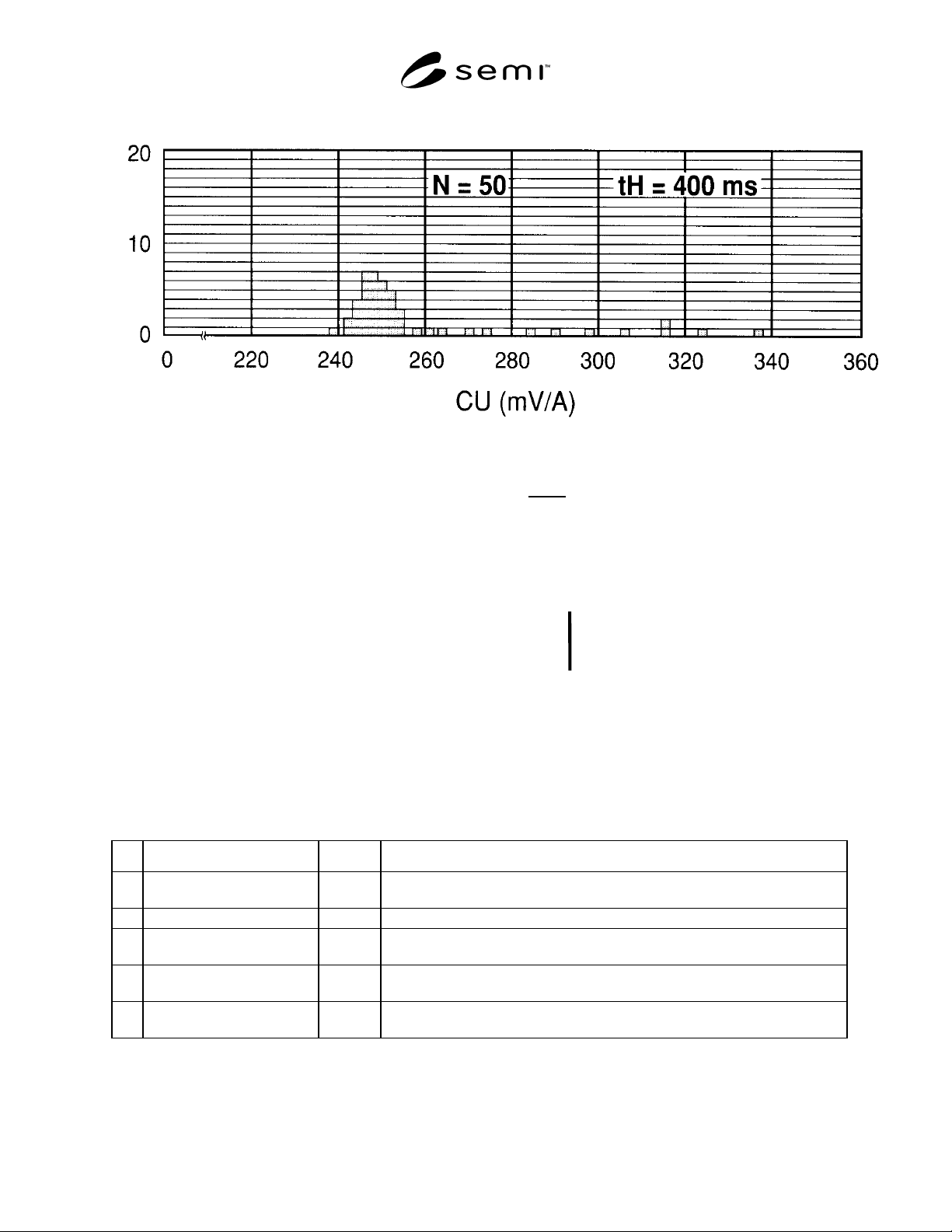
SEMI G46-88 © SEMI 1988 9 V = 5.0 v T = 400 m s I = 1.0 mA t = 2 0 CU = 249 mV/A σ = 53. 5 mV/A CU = 302. 5 m V/A H H M MD cu hig h lim it Figure 8 CU bar graph shows th er mal dis tribution of 50 dev ices when test ed a…
SEMI G46-88 © SEMI 1988 8
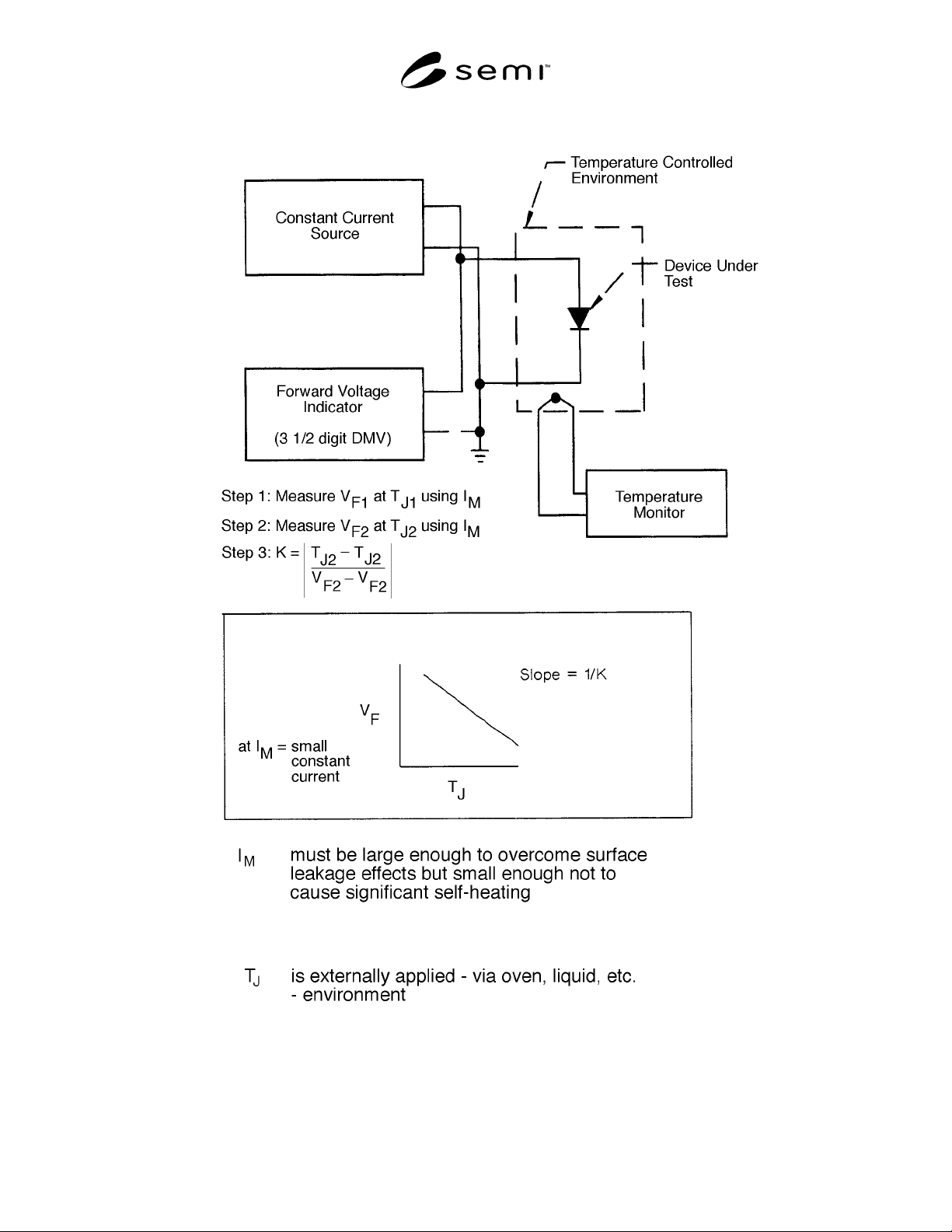
Figure 7
K Factor Calibration Setup and Procedure
SEMI G46-88 © SEMI 19889
V = 5.0 v
T = 400 ms
I = 1.0 mA
t = 20
CU = 249 mV/A
σ
= 53.5 mV/A
CU = 302.5 mV/A
H
H
M
MD
cu
high
limit
Figure 8
CU bar graph shows thermal distribution of 50 devices when tested at a heating time of 400 ms. (Note: CU data
rounded off to nearest m V/A.)
General Description Steps Comments
A Initial Setup 1 thru 4 Approximate instrument settings to find variations among devices in 10 to 15
piece sample.
B Heating Curve Generation 5 thru 7 Using highest and lowest reading devices, generate Heating Curves.
C Heating Curve Interpretation 8 thru 10 Heating Curve is used to find more appropriate value for t
H
corresponding to heat
in the die attachment are (or some other desired interface in the heat flow path).
D Final Setup 11 Heating Power applied during t
H
is increased in order to improve measurement
sensitivity to variations among devices.
E Pass/F Determination 12 thru 13 A variety of methods is available for setting the fail limit; the statistical approach
is the fastest and easiest to implement.
Figure 9 — Summary table of steps required to implement thermal transient testing for IC die attachment
evaluation.

SEMI G46-88 © SEMI 1988 10
NOTICE: These standards do not purport to address
safety issues, if any, associated with their use. It is the
responsibility of the user of these standards to establish
appropriate safety and health practices and determine
the applicability of regulatory limitations prior to use.
SEMI makes no warranties or representations as to the
suitability of the standards set forth herein for any
particular application. The determination of the
suitability of the standard is solely the responsibility of
the user. Users are cautioned to refer to manufacturer’s
instructions, product labels, product data sheets, and
other relevant literature respecting any materials
mentioned herein. These standards are subject to
change without notice.
The user’s attention is called to the possibility that
compliance with this standard may require use of
copyrighted material or of an invention covered by
patent rights. By publication of this standard, SEMI
takes no position respecting the validity of any patent
rights or copyrights asserted in connection with any item
mentioned in this standard. Users of this standard are
expressly advised that determination of any such patent
rights or copyrights, and the risk of infringement of such
rights, are entirely their own responsibility.
Copyright by SEMI® (Semiconductor Equipment and Materials
International), 3081 Zanker Road, San Jose, CA 95134. Reproduction o
f
the contents in whole or in part is forbidden without express written
consent of SEMI.