semi合集-English.pdf - 第7689页
SEMI T7-0303 © SEMI 1997, 2003 2 4.1.10 dat a matrix c ode symbol — a two-dim ensional array of squ are cells arranged in co ntiguous rows and columns. In cert ain ECC200 sym bols, data regions are separated by al ignmen…
SEMI T7-0303 © SEMI 1997, 2003 1
SEMI T7-0303
SPECIFICATION FOR BACK SURFACE MARKING OF DOUBLE-SIDE
POLISHED WAFERS WITH A TWO-DIMENSIONAL MATRIX CODE
SYMBOL
This specification was technically approved by the Global Traceability Committee and is the direct
responsibility of the North American Traceability Committee. Current edition approved by the North
American Traceability Committee on November 22, 2002. Initially available at www.semi.org January 2003;
to be published March 2003. Originally published in 1997; previously published November 2002.
1 Purpose
1.1 This specification is intended to provide a marking
symbology that can be used to mark silicon wafers with
no intrusion into the fixed quality area of the wafer.
2 Scope
2.1 This specification defines the geometric and spatial
relationships and content (including the error checking
and correcting code) of a rectangular two-dimensional
(2-D), machine-readable, binary data matrix code
symbol for back surface marking of notched, double-
side polished wafers of silicon which comply with
SEMI M1.15, and other materials with diameters of 300
mm and larger.
2.2 Although this specification does not specify the
marking techniques that may be employed when
complying with its requirements, it is assumed that the
symbol will be obtained by laser scribing individual
dots.
2.3 The matrix code is applicable to a broad range of
wafer products including epitaxial wafers, SOI wafers,
and unpatterned or patterned polished wafers. The
format and algorithms of this code are based on two-
dimensional symbology specified in ISO/IEC 16022.
NOTICE: This standard does not purport to address
safety issues, if any, associated with its use. It is the
responsibility of the users of this standard to establish
appropriate safety health practices and determine the
applicability or regulatory limitations prior to use.
3 Referenced Standards
3.1 SEMI Standards
SEMI AUX001 — List of Vendor Identification Codes
SEMI M1.15 — Standard for 300 mm Polished
Monocrystalline Silicon Wafers (Notched)
SEMI M12 — Specification for Serial Alphanumeric
Marking of Silicon Wafers
3.2 ISO/IEC Standard
1
ISO/IEC 16022 — International Symbology
Specification – Data Matrix
NOTICE: Unless otherwise indicated, all documents
cited shall be the latest published versions.
4 Terminology
4.1 Definitions
4.1.1 alignment bar, of a data matrix code symbol — a
solid line of contiguous filled cells abutting a line of
alternately filled and empty cells [ISO/IEC 16022].
4.1.2 binary values — a dot in the wafer surface
indicates the binary value 1. The absence of a dot, or a
smooth surface surrounding a cell center point indicates
the binary value 0.
4.1.3 border column — the outermost column of a data
matrix code symbol. This column is a portion of the
finder pattern.
4.1.4 border row — the outermost row of a data matrix
code symbol. This row is a portion of the finder pattern.
4.1.5 cell, of a data matrix code symbol — the area
within which a dot may be placed to indicate a binary
value.
4.1.6 cell center point, of an array — the point at
which the centerline of a row intersects the centerline of
a column.
4.1.7 cell spacing, of an array — the (equal) vertical or
horizontal distance between the cell center points of
contiguous cells.
4.1.8 center line, of a row or column — the line
positioned parallel to, and spaced equally between, the
boundary lines of the row or column.
4.1.9 central area, of a cell — the area enclosed by a
circle centered at the cell center point; used by code
readers to sense the binary value of the cell.
1 International Organization for Standardization, ISO Central
Secretariat, 1, rue de Varembé, Case postale 56, CH-1211 Geneva 20,
Switzerland. Telephone: 41.22.749.01.11; Fax: 41.22.733.34.30
Website: http://www.iso.ch
SEMI T7-0303 © SEMI 1997, 2003 2
4.1.10 data matrix code symbol — a two-dimensional
array of square cells arranged in contiguous rows and
columns. In certain ECC200 symbols, data regions are
separated by alignment patterns. The data region is
surrounded by a finder pattern [ISO/IEC 16022].
4.1.11 dot — a localized region with a reflectance
which differs from that of the surrounding surface.
NOTE 1: To assure reading efficiency, a minimum contrast
of 30% is required between the reflectance value of a dot and
the surrounding wafer surface. Various densitometers can
provide such measurements nondestructively.
4.1.12 dot misalignment, within a cell — the distance
between the physical center point of a dot and the cell
center point.
4.1.13 finder pattern, of a data matrix code symbol —
a perimeter to the data region. Two adjacent sides
contain dots in every cell; these are used primarily to
define physical size, orientation and symbol distortion.
The two opposite sides are made up of cells containing
dots in alternate cells [ISO/IEC 16022].
4.1.14 reference point, of a data matrix code symbol —
the physical center point of a corner cell common to the
primary border row and the solid line of the alignment
bar, used to identify the physical location of the symbol
on the object being marked with the symbol.
NOTE 2: The reference point is at a fixed location on the
object. Different cells may be chosen as the reference point
depending on the desired orientation of the symbol on the
object and the size variability of the symbol. The particular
cell to be used as the reference point must be specified for
each application.
5 Requirements
5.1 Shape and Size of the Data Matrix Code Symbol
5.1.1 Data Matrix Code Symbol Dimensions
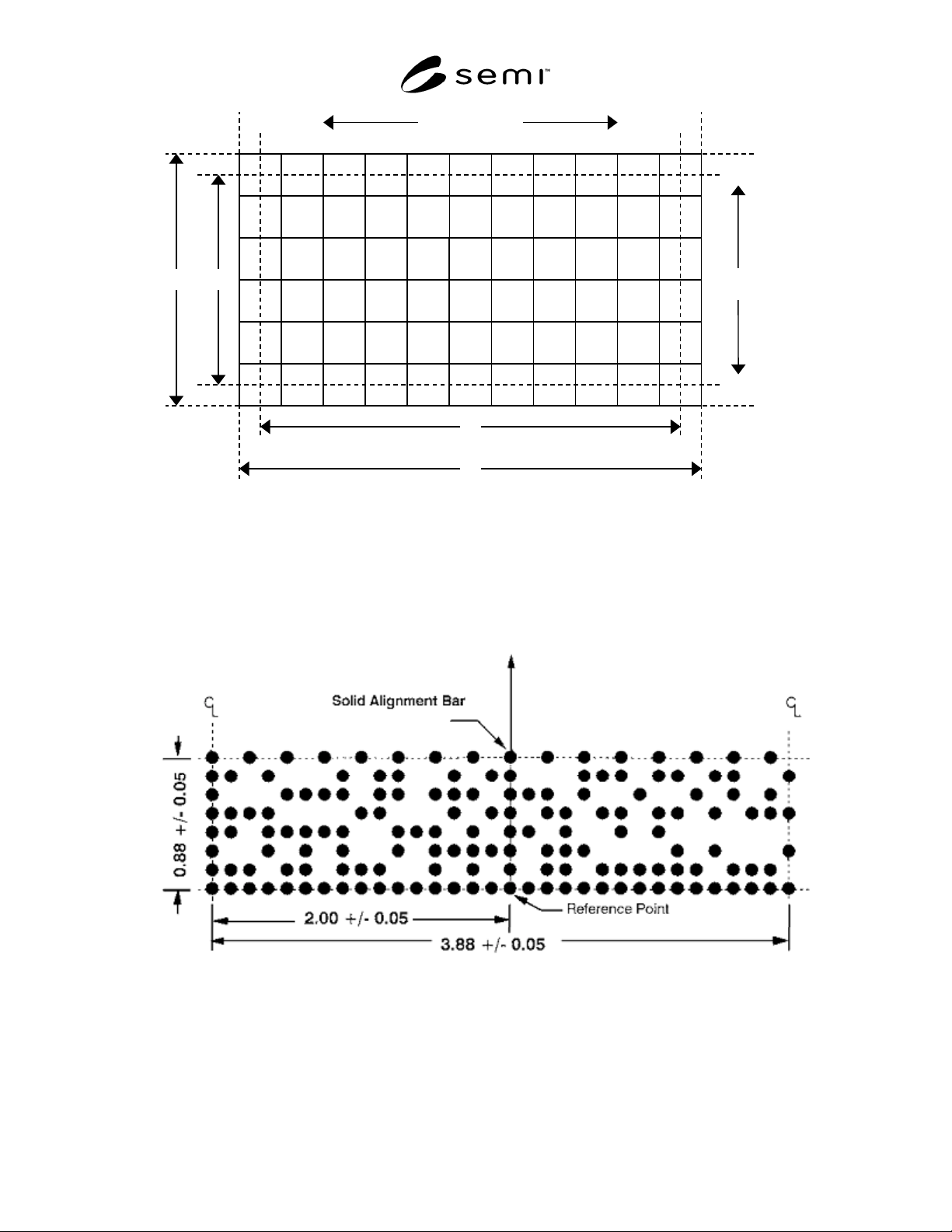
5.1.1.1 Each rectangular matrix code symbol shall be
composed of an array of 8 rows and 32 columns with an
alignment bar as defined in ISO/IEC ISS 16022.
5.1.1.2 Cell spacing shall be 125 µ m, center to center.
5.1.2 Dot Size — The nominal shape of the dot
produced in the matrix may be circular or square. Its
diameter or edge length (after polishing) shall be 100
µ m + 10 µ m – 20 µ m.
5.1.3 Border Rows and Columns
5.1.3.1 One border row and one border column shall
contain a dot in each cell. These are identified as the
primary border row and the primary border column.
These are used by the code reader to determine the
orientation of the matrix.
5.1.3.2 The opposing (secondary) border row and
column shall contain dots in alternating cells.
5.1.3.3 For these rectangular matrix code symbols, the
reference point of the symbol shall be the physical
centerpoint of the cell common to the primary border
row and the center alignment bar.
5.1.4 The maximum dot misalignment within a cell is
15 µ m. This ensures that a minimum size dot covers a
cell central area of radius 25 µ m.
5.1.5 Adjacent dots shall not touch.
5.2 Content of the Data Matrix Code Symbol
5.2.1 Each rectangular matrix code symbol shall
contain 10 message characters, together with the error
checking and correcting (ECC200) code characters,
encoded in accordance with ISO/IEC ISS 16022.
5.2.2 The message characters may include the
following: A–Z, 0–9, and dash (–). These characters
constitute the SEMI OCR Character Set except for the
period (.); this is the same character set specified in
SEMI M12. These characters are also included in the
set designated as “primarily upper case alphanumeric”
in ISO/IEC 16022, in Table 5 and Annexe J. The ten
message characters shall contain two elements:
a. a vendor-assigned 8-character wafer identification
code, followed by
b. a 2-character vendor identification code (see SEMI
AUX001).
5.3 Location of the Data Matrix Code Symbol
5.3.1 With the wafer positioned back surface up and
with the primary fiducial (notch) toward the operator,
the origin of the data matrix code symbol shall be
located as specified below.
5.3.1.1 The 8 row × 32 column rectangular 2-D matrix
code symbol shall be placed entirely outside a fixed
quality area (FQA) with a nominal edge exclusion of 3
mm. The reference point shall be located 148.95 ± 0.15
mm from the center of the wafer, along a radius 5.0 ±
0.1° counterclockwise from the axis of the notch
fiducial bisector.
5.3.2 The primary row of the matrix code symbol shall
be placed toward the periphery of the wafer.
SEMI T7-0303 © SEMI 1997, 2003 3
32 cells per row
C1 C2
R1
R2
8 cells per
column
Nominal Dimensions (mm)
R1 = 3.875
C1 = 0.875
R2 = 4.000
C2 = 1.000
C
L
C
L
C
L
C
L
Figure 2
Data Matrix Field Dimensions
ECC200 - 8 rows × 32 columns
To Wafer Cente
r
Dimensions in millimeters are o
f
center to center of dots
Figure 3
Data Matrix Code Fields
ECC200 - 8 rows × 32 columns