semi合集-English.pdf - 第4464页
SEMI D16-0998 © SEM I 1998 3 Figure 1B Proposed T ransport System to Tool In terface 6.2 Centerline location of the subs t r a te, as it is delivered by the material handling equipment, w ith respect to the tool face m a…
SEMI D16-0998 © SEMI 1998 2
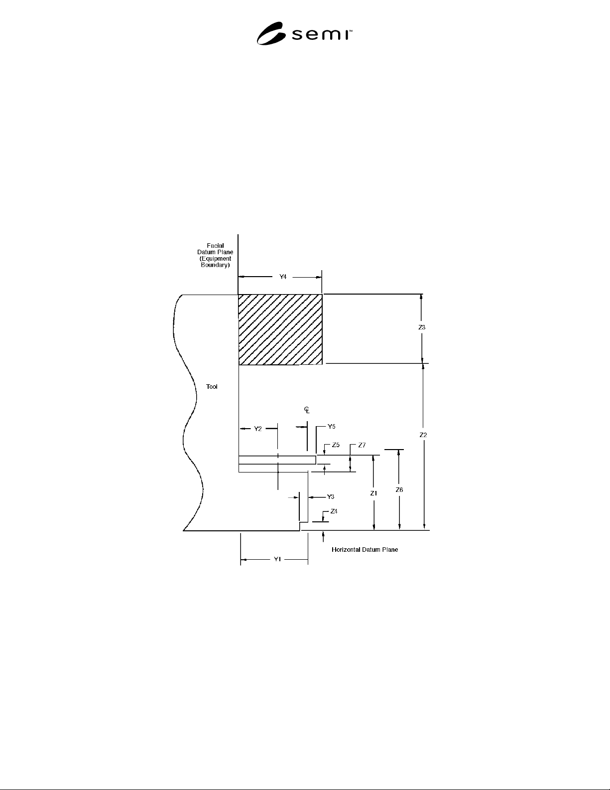
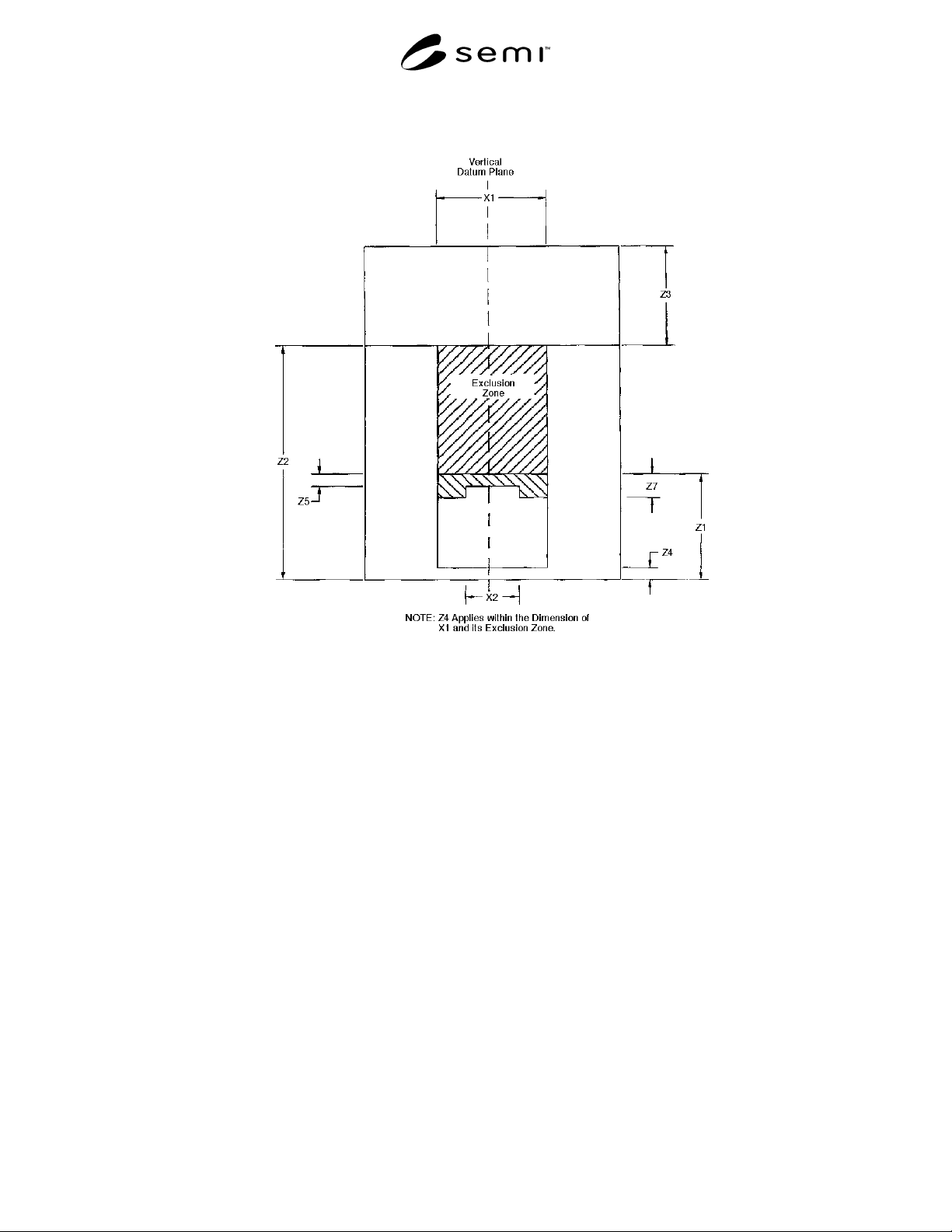
5.2.11 Z4 — the height of the exclusion zone used for PGV cart alignment devices.
5.2.12 Z5 — the maximum height of the protrusion used for docking devices.
5.2.13 Z6 — the location for the bottom plane of the first substrate. This dimension is not specified in this
document.
5.2.14 Z7 — height of exclusion zones used by conveyor rails and fork lifts; maximum.
6 Requirements
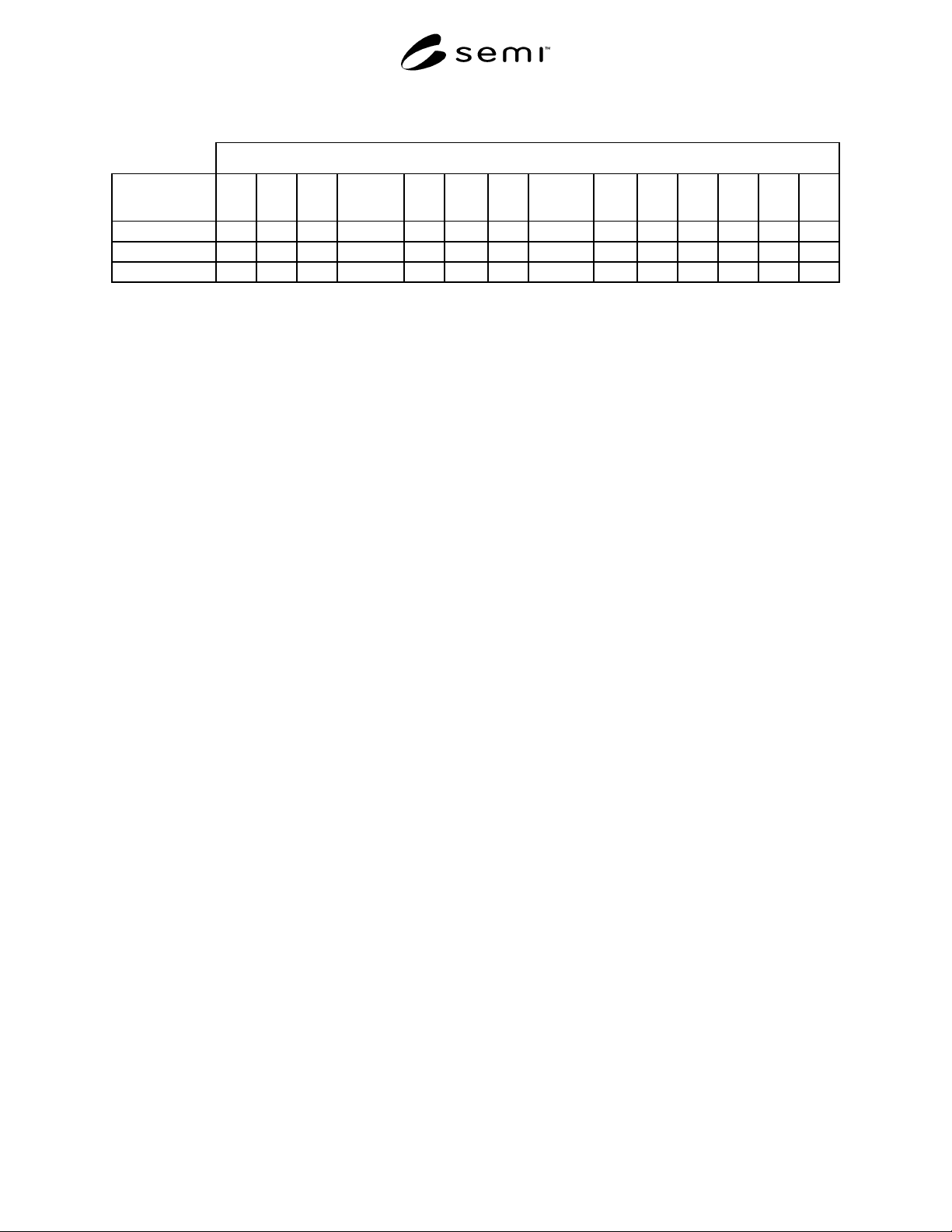
6.1 Dimensions and tolerances of the required features are specified in Table 1 and Figures 1A and 1B.
Figure 1A
Proposed Transport System to Tool Interface
SEMI D16-0998 © SEMI 19983
Figure 1B
Proposed Transport System to Tool Interface
6.2 Centerline location of the substrate, as it is delivered by the material handling equipment, with respect to the
tool face may not coincide with the centerline location of the substrate when the latter is finally positioned on the
tool port for substrate handling.
6.3 Substrate delivery is to be horizontal, active (pattern) face up.
6.4 The single substrate or carrier is to have a horizontal loading orientation with shorter side parallel to the tool
face plane.
6.5 Load height of the single substrate or carrier shall be adjustable on the material handling system within 20 (±
10) mm of the nominal height.
6.6 There should be no obstruction between the load port and the material delivery system within the defined
adjustable range of the load port height.
6.7 Load and unload mechanisms must allow operator-assisted loading. This implies clearance space for the
operator, as well as mechanisms that allow manual override.
SEMI D16-0998 © SEMI 1998 4
Table 1 Substrate Edge Length, Interface Dimensions, and Tolerances (mm)
Interface Dimensions and Tolerances
Edge Length
(mm)
X1
max.
X2
max.
Y1
max.
Y2
± 10 mm
Y3
max.
Y4
max.
Y5
max.
Z1
± 10 mm
Z2
min.
Z3
max.
Z4
max.
Z5
max.
Z6 Z7
max.
550 × 650 925 450 800 400 100 1000 100 900 2000 850 100 105 tba 200
600 × 720 980 500 865 435 100 1065 100 900 2000 850 100 105 tba 200
960 × 1100 1450 900 1360 650 100 1500 100 900 2000 850 100 105 tba 200
NOTICE: These standards do not purport to address safety issues, if any, associated with their use. It is the
responsibility of the user of these standards to establish appropriate safety and health practices and determine the
applicability of regulatory limitations prior to use. SEMI makes no warranties or representations as to the suitability
of the standards set forth herein for any particular application. The determination of the suitability of the standard is
solely the responsibility of the user. Users are cautioned to refer to manufacturer's instructions, product labels,
product data sheets, and other relevant literature respecting any materials mentioned herein. These standards are
subject to change without notice.
The user's attention is called to the possibility that compliance with this standard may require use of copyrighted
material or of an invention covered by patent rights. By publication of this standard, SEMI takes no position
respecting the validity of any patent rights or copyrights asserted in connection with any item mentioned in this
standard. Users of this standard are expressly advised that determination of any such patent rights or copyrights, and
the risk of infringement of such rights, are entirely their own responsibility.
Copyright by SEMI® (Semiconductor Equipment and Materials
International), 3081 Zanker Road, San Jose, CA 95134. Reproduction o
f
the contents in whole or in part is forbidden without express written
consent of SEMI.