semi合集-English.pdf - 第5982页
SEMI P42-0304 © SEMI 2004 15 </WaferInfor mation> <ShotMapInform ation> <StepPitch> <X>20000</X> <Y>20000</Y> <UnitType>um</UnitType> < / S t e p P i t c h > &l…
SEMI P42-0304 © SEMI 2004 14
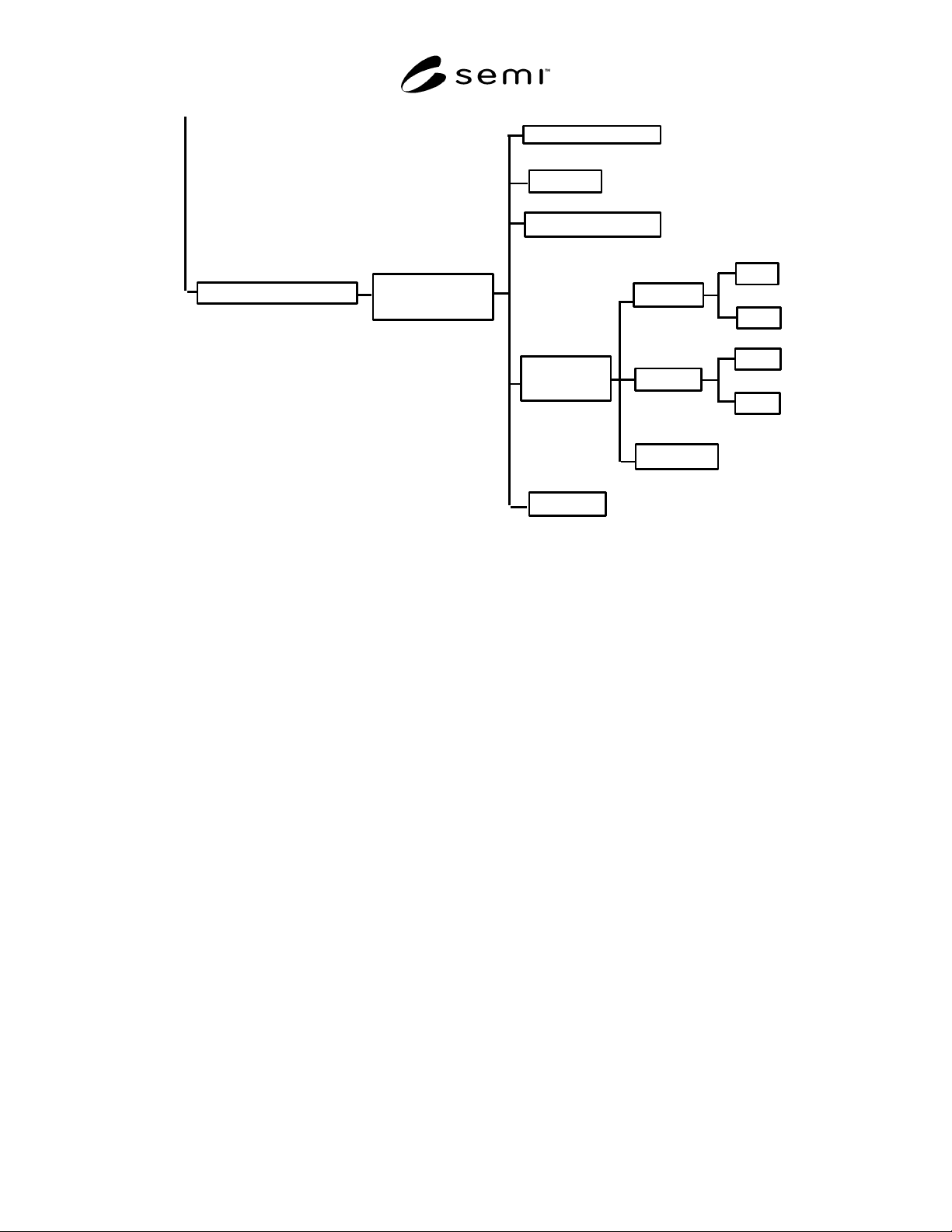
Alignment USE Mark
AlignmentMark
Information
Comment
WaferMarkType
Group
Ali
g
nmentMarkID
Wa
f
erMark
Position
Y
X
X-Mark
Y
X
Y-Mark
Unit Type
R1-2 XML Description Sample
This sample is provided with the repetitive description of <ShotID>S76 from <ShotID>S9 not repeated.
<?xml version="1.0" encoding="UTF-8"?>
<rfd:rdm xmlns:rfd="file://XML\SEMI_Samples\SemiSEMI" xmlns:xsi="http://www.w3.org/2001/XMLSchema-
instance" xsi:schemaLocation="file://XML\SEMI_Samples\SemiSEMI
C:\XML\SEMI_Samples\SEMIReticleFlameData.xsd">
<FormulationInformation>
<Date>2003-12-03T13:20:00+08:00</Date>
<Person>H.HIGASHINO</Person>
</FormulationInformation>
<UseExposureMachine>
<MachineTypeInformation>NSR-xxxxxx</MachineTypeInformation>
</UseExposureMachine>
<ShotMap>
<WaferInformation>
<WaferType>SEMI/notch</WaferType>
<WaferSize>
<Size>8</Size>
<UnitType>inch</UnitType>
</WaferSize>
<EdgeClearance>
<Clearance>3</Clearance>
<UnitType>mm</UnitType>
</EdgeClearance>
<WaferThickness>
<Thickness>725</Thickness>
<UnitType>um</UnitType>
</WaferThickness>
<WaferRotation>0</WaferRotation>
SEMI P42-0304 © SEMI 2004 15
</WaferInformation>
<ShotMapInformation>
<StepPitch>
<X>20000</X>
<Y>20000</Y>
<UnitType>um</UnitType>
</StepPitch>
<ShotMapArray>
<C>10</C>
<R>9</R>
</ShotMapArray>
<ShotMapOffset>
<X>0</X>
<Y>-1250</Y>
<UnitType>um</UnitType>
</ShotMapOffset>
</ShotMapInformation>
<ShotAreaInformation>
<ShotAreaID>AREA-A</ShotAreaID>
<ReticleID>RET-G</ReticleID>
<ShotAreaSize>
<X>20100</X>
<Y>20100</Y>
<UnitType>um</UnitType>
</ShotAreaSize>
<ShotAreaShift>
<X>0</X>
<Y>0</Y>
<UnitType>um</UnitType>
</ShotAreaShift>
<ShotAreaPositionShift>
<X>0</X>
<Y>0</Y>
<UnitType>um</UnitType>
</ShotAreaPositionShift>
</ShotAreaInformation>
<ShotInformation>
<ShotID>S1</ShotID>
<ShotAreaID>AREA-A</ShotAreaID>
<ShotLocation>
<C>3</C>
<R>1</R>
</ShotLocation>
<ShotPosition>
<X>-50000</X>
<Y>78750</Y>
<UnitType>um</UnitType>
</ShotPosition>
</ShotInformation>
<ShotInformation>
<ShotID>S2</ShotID>
<ShotAreaID>AREA-A</ShotAreaID>
<ShotLocation>
<C>4</C>
<R>1</R>
</ShotLocation>
SEMI P42-0304 © SEMI 2004 16
<ShotPosition>
<X>-30000</X>
<Y>78750</Y>
<UnitType>um</UnitType>
</ShotPosition>
</ShotInformation>
<ShotInformation>
<ShotID>S3</ShotID>
<ShotAreaID>AREA-A</ShotAreaID>
<ShotLocation>
<C>5</C>
<R>1</R>
</ShotLocation>
<ShotPosition>
<X>-10000</X>
<Y>78750</Y>
<UnitType>um</UnitType>
</ShotPosition>
</ShotInformation>
<ShotInformation>
<ShotID>S4</ShotID>
<ShotAreaID>AREA-A</ShotAreaID>
<ShotLocation>
<C>6</C>
<R>1</R>
</ShotLocation>
<ShotPosition>
<X>10000</X>
<Y>78750</Y>
<UnitType>um</UnitType>
</ShotPosition>
</ShotInformation>
<ShotInformation>
<ShotID>S5</ShotID>
<ShotAreaID>AREA-A</ShotAreaID>
<ShotLocation>
<C>7</C>
<R>1</R>
</ShotLocation>
<ShotPosition>
<X>30000</X>
<Y>78750</Y>
<UnitType>um</UnitType>
</ShotPosition>
</ShotInformation>
<ShotInformation>
<ShotID>S6</ShotID>
<ShotAreaID>AREA-A</ShotAreaID>
<ShotLocation>
<C>8</C>
<R>1</R>
</ShotLocation>
<ShotPosition>
<X>50000</X>
<Y>78750</Y>
<UnitType>um</UnitType>