semi合集-English.pdf - 第4439页
SEMI D9-0303 © SEMI 1994, 2003 3 orientation corner X Y corner cut (3 places) Figure 2 Orientation Corner and Corner Cut 4.4.10 squareness dev iation of the outline of the substrate from a true square or rectangle. Usi…
SEMI D9-0303 © SEMI 1994, 2003 2
4.2.3 stain organic or inorganic material on the
surface.
4.2.4 blur — any erosion of the surface; generally
cloudy in appearance, it sometimes exhibits an apparent
color.
4.3 Surface Defects
4.3.1 scratch
a surface fissure generally caused
during handling.
4.3.2 sleek — a very shallow type of scratch on the
polished surface that is sometimes invisible when the
viewing angle is changed.
4.3.3 latent scratch — a scratch which is usually
invisible but when subjected to an etching action by
dipping into a detergent or a corrosive solution, such as
an acid, the previously invisible scratch becomes visible
due to the minor removal of surface glass.
4.3.4 chip — a region of material missing from the
edge of the glass substrate, which is sometimes caused
by processing or handling.
4.3.5 pit/dig — small indentation on the glass substrate
surface.
4.3.6 bump a small protuberance on the glass
substrate.
4.3.7 crack — a fissure located at the sheet edge area
or central area.
4.3.8 streak — a defect with a very small undulation
on the glass substrate surface.
4.4 Dimensional Properties
4.4.1 outsize dimension vertical and horizontal
dimensions of the glass substrate.
4.4.2 thickness
the distance between the front
surface and the back surface of a glass substrate at same
single point.
4.4.3 thickness variation — any differences between
maximum and minimum values within the thickness of
a glass substrate.
4.4.4 warp defined as the maximum distance from a
reference plane to the guaranteed surface; this includes
twists, partial rises or declines in the glass compared
with the reference plane. Warp expression a condition
of the whole glass (substrate).
4.4.5 waviness the residual unevenness after the
long wavelength component (warp) and the short
wavelength component (surface roughness) have been
eliminated. This is also called “FPD Waviness” when
referring specifically to FPD substrates, as in SEMI
D15.
4.4.6 surface roughness — the criterion for the
smoothness of the sheet surface. Usually the randomly
selected areas on the sheet surface are measured by a
surface analyzer. Details are defined in SEMI D7.
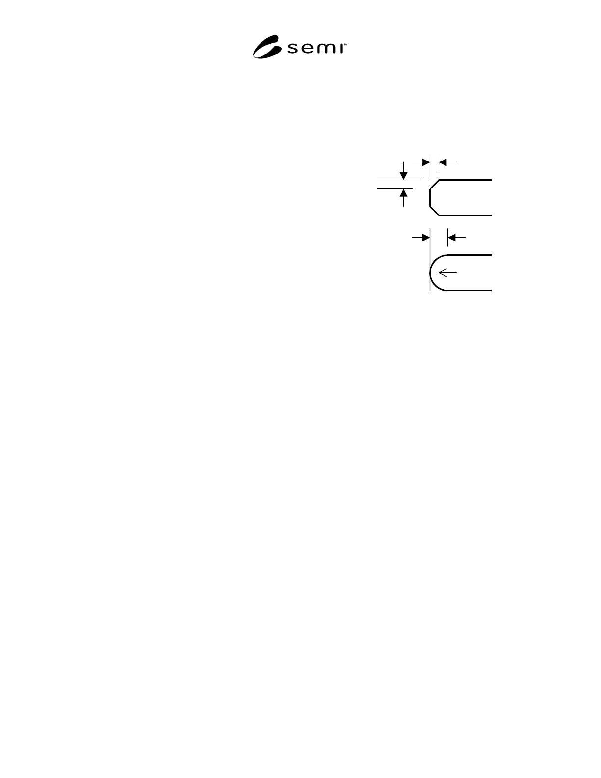
4.4.7 beveling grinding out or shaping substrate
edges by lapping or grinding.
X
Y
chamfered edge
radiused edge
R
W
Figure 1
Beveling
4.4.7.1 chamfered edge a beveled angle of
approximately 45° in respect to the surface and cut edge
surface. One characteristic is that part of the cut edge
surface remains. For this reason, R-beveled edges have
come to be used in conjunction with chamfered edges
in liquid crystal applications. Chamfered edges with
particularly small widths are also referred to as “string
bevels”. (See Figure 1.)
4.4.7.2 R beveled edge — a beveled shape of an arc in
respect to the surface and cut edge surface. One
characteristic is that the complete cut edge surface is
ground with a wheel and processed into a frosted glass
state. Generally, in TFT liquid crystals, R-beveled
edges are used more often. (See Figure 1.)
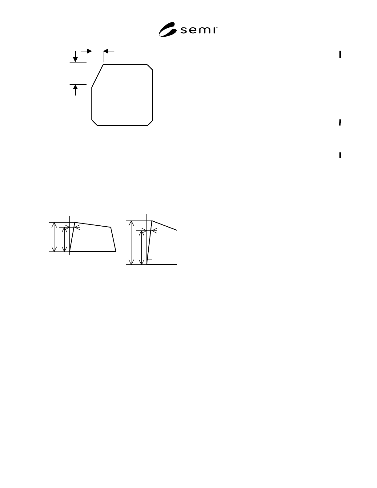
4.4.8 orientation corner — the corner of a substrate
which identifies the pattern surface and the rotational
orientation. It is defined by the X and Y dimensions in
the following figure. It is also commonly known as
“orientation flat” or “orifra”.
4.4.9 corner cut — removal of the corners of the
substrate by either lapping or grinding. As with the
orientation corner, this is defined by the X and Y
dimensions, but generally, most corner cuts have a X
and Y of the same length.
SEMI D9-0303 © SEMI 1994, 2003 3
orientation
corner
X
Y
corner cut
(3 places)
Figure 2
Orientation Corner and Corner Cut
4.4.10 squareness deviation of the outline of the
substrate from a true square or rectangle. Using the
drawing below, it is defined as PS or PL, but must be
recorded with a or b dimensions. Dimensions a and b
can be decided voluntarily, but generally, most
applications use a = S and b = L. (See Figure 3.)
a
P
S
L
≥
S
b
L
P
L
S
Figure 3
Squareness
4.5 Thermal Properties
4.5.1 coefficient of thermal expansion expansion is
the change in length per initial length caused by a
thermal change. Concretely, it is shown as ∆L/L0,
where ∆L = L2 – L1 and L0, L1, and L2 are the lengths
of the material at the temperature T0, T1, T2
respectively. Usually, the coefficient of expansion (A),
means the average coefficient of expansion over the
temperature range T1 to T2. This is shown in the
following equation.
α
= (∆L/∆T)/L
0
= [(L
2
–
L
1
)/(T
2
–
T
1
)]/L
0
4.5.2 thermal shrinkage when the substrate is heat
treated along a specific thermal profile, the relaxation
of thermal stress and the structure change occur in
material, and create the shrinkage of the substrate.
Usually it is described with ∆L/L0, where, ∆L is the
amount of change and shown as ∆L = L0 – L. L0 is the
length of material before heat treatment, and L is after
heat treatment.
4.5.3 strain point temperature of the glass when its
viscosity is approximately 10
14..5
dPa·s. Strain point is
defined by two methods in ASTM: Test Method C336
(Elongation of Glass Fibers) and Test Method C598
(Bending in Glass Beams). In practice, the strain point
of glass is the maximum temperature at which glass can
be processed without triggering unnecessary strain.
Internal strain can be relieved by keeping (the glass) at
this temperature for 4 hours.
4.5.4 annealing point temperature of the glass when
its viscosity is approximately 10
13
dPa·s. The annealing
point is the temperature at which internal strain can be
relieved in 15 minutes.
4.5.5 softening point temperature of the glass when
its viscosity is approximately 10
7.6
dPa·s. Softening
point is defined in ASTM C338.
4.6 Chemical Properties
4.6.1 chemical durability a measure of corrosion or
attack of a glass surface when subjected to a specific
reagent, such as acid, base, or water at a specific
concentration for a specific time and temperature.
4.7 Optical Properties
4.7.1 transmittance — percentage of incident light
which permeates the glass. It is defined as I/Io, where
Io is the strength of the incident light, and I is strength
of the permeated light. Transmittance is effected by
material composition, temperature, thickness and light
wavelength.
4.7.2 refractive index — ratio of the speed of light in
the material and in a vacuum at a specific wavelength.
The refractive index of substrate glass is between
approximately 1.50 and 1.53.
4.8 Mechanical Properties
4.8.1 density
mass per unit volume. Decided by the
mass of the material’s atomic composition and the
volume (comparative capacity, mol capacity) which it
occupies.
4.8.2 Young’s modulus
a type of elasticity ratio,
which shows the stretch (or compression) elasticity.
When stretch (or compression) deformation stress σ and
the strain ε resulting from the stress are proportionate,
the proportionate constant E = σ/ ε is called Young’s
modulus, a material characteristic.
4.8.3 shear modulus a type of elasticity ratio which
shows divergence elasticity. When divergent
deformation stress τ and the strain Φ resulting from the
stress are proportionate, the proportionate constant
G = τ/Φ is called Shear Modulus, a material
characteristic.
SEMI D9-0303 © SEMI 1994, 2003 4
4.8.4 Poisson’s ratio the ratio between Young’s
modulus and shear modulus.
4.8.5 Vickers hardness — a type of pressure test. A
diamond pyramid indentator with a face angle of 136°
is pressed into the glass surface to find the degree of
hardness by measuring trace indentation on the overall
squareness.
4.9 Electrical Properties
4.9.1 dielectric constant the proportionate dielectric
constant which is the ratio between a vacuum dielectric
constant and the material dielectric constant.
4.9.2 dielectric loss — the phenomenon, or volume, of
(electricity) loss through heat when a dielectric is
introduced to an alternating current.
4.9.3 resistivity — the reciprocal of electric
conductivity.
4.10 pattern surface — the main area where device
patterns can be formed, determined by the orientation
corner, etc.
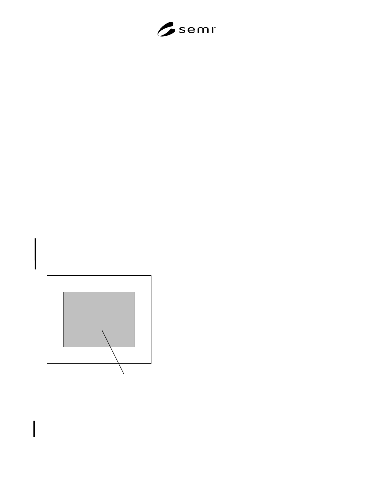
4.11 quality area — the center area to the substrate
where specified substrate quality criteria (primarily
internal defects, surface contamination, surface defects,
waviness, and surface roughness) are applicable.
5 Referenced Documents
SEAJ(Semiconductor Equipment Association of Japan)
Liquid Crystal Display Manufacturing Equipment
Dictionary
2
quality area
Figure 4
Quality Area
2 Semiconductor Equipment Association of Japan, 7-10 Shinjuku 1-
chome, Shinjuku-ku, Tokyo, 160-0022 Japan. Tel:+81-3-3353-7589,
fax:+81-3-3353-7970, http://www.seaj.or.jp
NOTICE: SEMI makes no warranties or
representations as to the suitability of the standards set
forth herein for any particular application. The
determination of the suitability of the standard is solely
the responsibility of the user. Users are cautioned to
refer to manufacturer’s instructions, product labels,
product data sheets, and other relevant literature
respecting any materials mentioned herein. These
standards are subject to change without notice.
The user’s attention is called to the possibility that
compliance with this standard may require use of
copyrighted material or of an invention covered by
patent rights. By publication of this standard, SEMI
takes no position respecting the validity of any patent
rights or copyrights asserted in connection with any
item mentioned in this standard. Users of this standard
are expressly advised that determination of any such
patent rights or copyrights, and the risk of infringement
of such rights, are entirely their own responsibility.
Copyright by SEMI® (Semiconductor Equipment and Materials
International), 3081 Zanker Road, San Jose, CA 95134. Reproduction o
f
the contents in whole or in part is forbidden without express written
consent of SEMI.