semi合集-English.pdf - 第7230页
SEMI MF154-0305 © SEMI 2003, 2005 4 Figure 7 Epitaxial Stacking Faults on (100), No Prepar ation Required, Size Dependent Up on EPI Thickness Figure 8 Epitaxial Stacking Faults on (100), No Prepar ation Required, Size De…

SEMI MF154-0305 © SEMI 2003, 2005 3
5 Terminology
5.1 Terms related to silicon technology, including the features and contaminants discussed in this guide, are defined
in SEMI M59.
6 Procedure
6.1 Procedures for examining silicon wafers for the features and contaminants discussed in this guide are covered in
SEMI MF523, SEMI MF1725, SEMI MF1726, SEMI MF1727, SEMI MF1809, and SEMI MF1810.
7 Keywords
contaminant; defects; dislocation; epitaxial; fracture; preferential etch; scratch; shallow pit; silicon; slip; stacking
fault
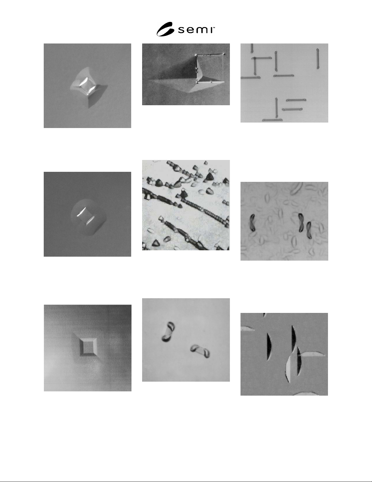
Figure 1
Dislocation Etch Pits on (111)
Silicon, Following 3-Min Sirtl
Etch, Magnification 110×
Figure 2
Dislocation Etch Pits on (110)
Silicon, Following 5-Min Wright
Etch, Magnification 110×
Figure 3
Dislocation Etch Pits on (100)
Silicon Following Schimmel (B)
Preferential Etch, Magnification
320×
Figure 4
Dislocation Etch Pits on (100)
Silicon Following Sirtl Etch,
Magnification 400×
Figure 5
Dislocation Etch Pits on (100)
Silicon Following 5-Min Wright
Etch, Magnification 200×
Figure 6
Epitaxial Stacking Faults on
(111) Following 4.2 m Dash etch,
Size Dependent Upon EPI
Thickness
SEMI MF154-0305 © SEMI 2003, 2005 4
Figure 7
Epitaxial Stacking Faults on
(100), No Preparation Required,
Size Dependent Upon EPI
Thickness
Figure 8
Epitaxial Stacking Faults on
(100), No Preparation Required,
Size Dependent Upon EPI
Thickness
Figure 9
Epitaxial Growth Hillock on
(100), No Preparation Required,
Size Dependent Upon EPI
Thickness
Figure 10
Epitaxial Stacking Faults on
(100), No Preparation Required,
Size Dependent Upon EPI
Thickness
Figure 11
Lineage on (111) Silicon
Following Preferential Etch,
Magnification 140×
Figure 12
Oxidation Induced Stacking
Faults on (100) Silicon Following
Oxidation and 4-min Wright
Etch, Magnification 200×
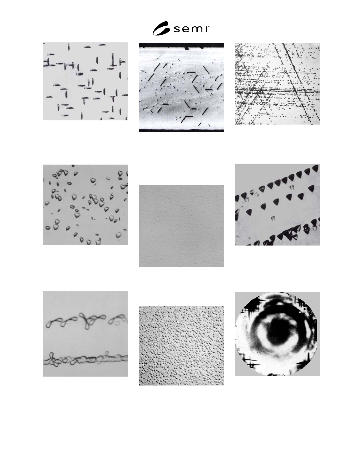
Figure 13
Oxidation Induced Stacking
Faults from Liquid Hone
Damage on a (100) Silicon
Polished Frontside Surface
Following Oxidation at 1100°C
and 1-min Schimmel Etch,
Magnification 1500×
Figure 14
Oxidation Induced Stacking
Faults from Liquid Hone
Damage on a (100) Etched Back
Surface Following Oxidation at
1100°C and 1-Min Schimmel
Etch, Magnification 1500×
Figure 15
Oxidation Induced Stacking
Faults on (100) Silicon Following
Oxidation and 3-Min Secco Etch,
Magnification 500×
SEMI MF154-0305 © SEMI 2003, 2005 5
Figure 16
Oxidation Induced Stacking
Faults on (100) Silicon Following
Oxidation and 3-min Secco Etch,
Magnification 200×
Figure 17
Oxidation Induced Stacking
Faults on (111) Silicon Following
Oxidation and 4-min Wright
Etch, Magnification 200×
Figure 18
Oxidation Induced Stacking
Faults Caused by a Scratch on
(100) Silicon Following Oxidation
and 2-min Wright Etch,
Magnification 400×
Figure 19
Oxidation Induced Stacking
Faults and Precipitates Found on
the Cleavage Face of a Silicon
Wafer After Thermal Treatment
and 3-min Secco Etch,
Magnification 100×
Figure 20
Relatively Small Shallow Pits on
(111) Following Oxidation and
4-min Wright Etch,
Magnification 200×
Figure 21
Relatively Large Shallow Pits on
(111) Following Oxidation and
4-min Wright Etch,
Magnification 200×
Figure 22
Slip on a (111) Preferentially
Etched Wafer, Magnification 5×
Figure 23
Slip on a (111) Preferentially
Etched Wafer, Magnification
140×
Figure 24
Slip Lines on a (100) Wafer
Visible as a Cross Hatched
Pattern Near the Edge Because
Shallow Pits are Gettered
Following Oxidation and 4-min
Wright Etch