semi合集-English.pdf - 第4455页
3 SEMI D13-1101 © SEMI 1995, 20 01 8.8 r eflectance non-uniform ity — V a r iatio n in reflectance o f the surface of color filter within the quality area. 8.9 hill — A gently slo ping p roj ec t i o n sma ller t han t h…
SEMI D13-1101 © SEMI 1995, 2001 2
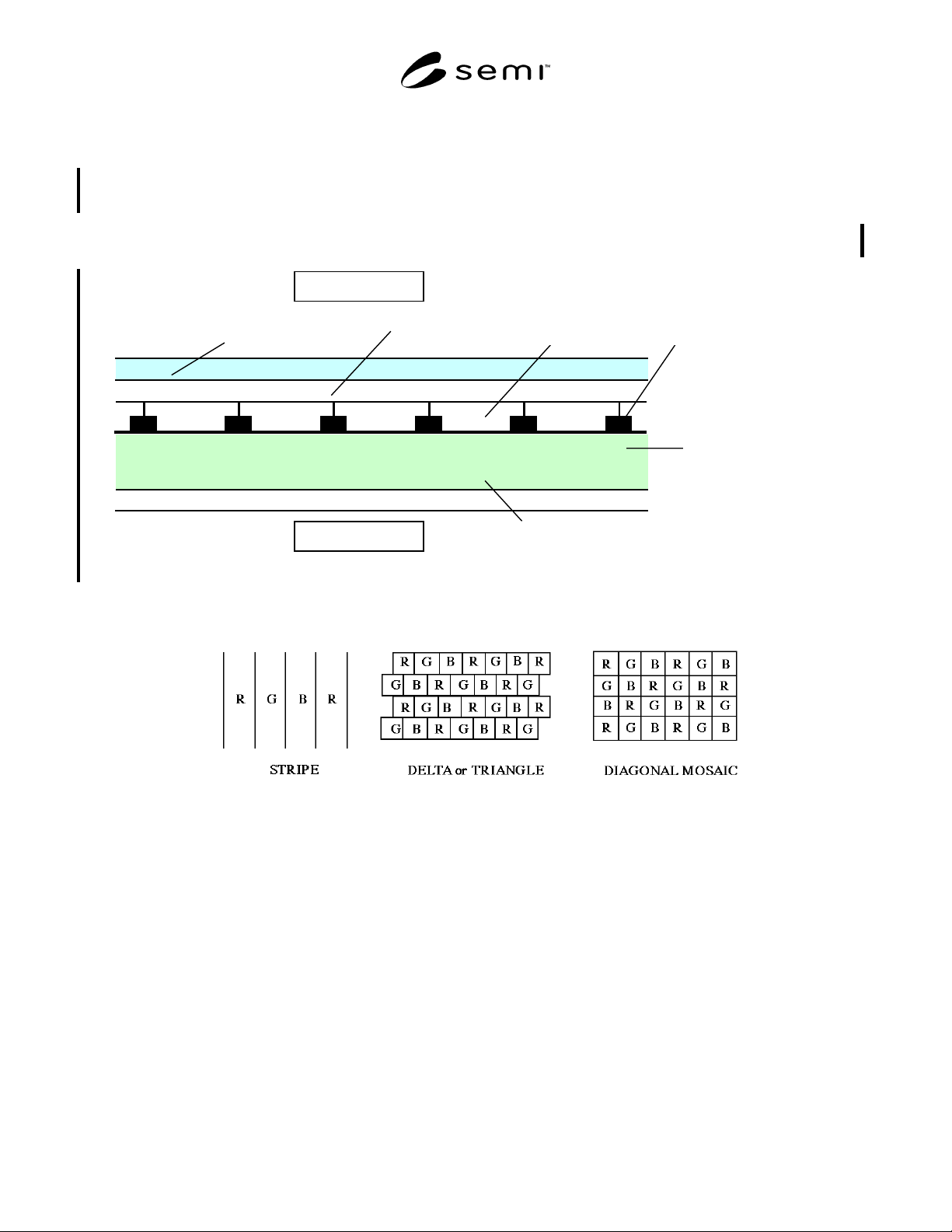
may vary to suit the application. These are illustrated in
Figure 2.
7 Color Filter Types and Fabrication Methods
7.1 Fabrication Methods
7.1.1 photolithography — Patterning method by using
micro photolithograph machines and photopatternable
materials. Precise patterns can be formed.
7.1.2 color photoresist method
Defined as color
photoresist, it is possible to create a pattern through a
direct exposure method using color pigment or dye
dispersed on a photoresist.
7.1.3 dyeing — Dyeable photoresist materials are
patterned by photolithographic image processing.
These patterned materials are dyed by a special method.
The various colors may be introduced sequentially.
7.1.4 etching — Dye or pigment-dispersed color
material is coated on substrate, and it is patterned by
photolithographic etching method.
7.1.5 printing — Pigment-dispersed color ink is placed
and patterned on the substrate by printing method.
7.1.6 electric deposition — Micro cells capsulating
pigment particles are dispersed in water solvent and
deposited on the selected electrode on glass substrate.
7.1.6.1 patterned ITO method
Color filter layers are
accumulated using a micell distribution liquid for each
color of the ITO pattern formed according to the
various RGB color filter layers.
7.1.6.2 resist pattern method
Color filter layers are
accumulated on non-patterned ITO film by using a
micell distribution liquid through openings (windows)
in the photoresist according to the RGB pattern.
7.1.7 multi-layer interference CF (Dichroic CF) —
Multiple layers of inorganic transparent thin films are
patterned by photolithography method.
7.1.8 ink jet method
Color filter layers are formed
by pigment or dye-colored ink blown out from an ink
jet head nozzle onto the substrate pixels.
7.1.9 others
Fabrication methods other than those
above.
7.2 coloring materials
Other than the multi-layer
interference method, these are formed using pigments
or dyes.
7.2.1 pigment
This can be pigment in fine powder
form dispersed into plastic, or it can be pigment in fine
powder form then capsulated in micell (microcell) and
dispersed in a water solution.
7.2.2 dye
Patterned plastic or gelatin is colored
using dye. Also, dyed plastic or gelatin can be patterned
using photolithography.
7.2.3 inorganic permeable thin film
A clear thin
film of inorganic material formed through methods
such as vacuum deposition or sputtering.
7.2.4 Other
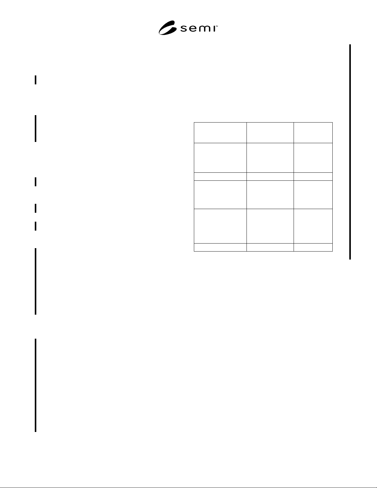
Table 1 Color Filter Fabrication Methods and
Materials
Fabrication Method
(main category)
Fabrication
Method
(subcategory)
Material
Photolithography Color Resist
Method
Dyeing Method
Etching Method
Pigment/Dye
Dye
Pigment/Dye
Printing Pigment
Electric Disposition Patterned-ITO
Method
Resist Pattern
Method
Pigment
Pigment
Mulit-layer
Interference
Vacuum
Evaporation
Method
Sputtering
Method
Inorganic
Material
Inorganic
Materials
Ink Jet Method Pigment/Dye
8 Visible Defects
8.1 black defect — Black dot-shaped defect existing in
the quality area that can be detected using transmitted
light.
8.2 white defect — White dot-shaped defect existing
in the quality area that can be detected using
transmitted light.
8.3 BM (Black Matrix) spot — A dot-shaped defect
caused by extraneous BM material deposited within the
quality area, not related to the BM pattern.
8.4 BM (Black Matrix) pin hole or pinhole — A dot-
shaped defect located within the BM pattern.
8.5 decolorant — The absence of a color element in a
normally tri-colored pixel. This may occur in a partial
area of one pixel.
8.6 color non-uniformity — Variation in brightness or
chromaticity within the quality area.
8.7 color spot — A mixing or overlapping of color
materials within an RGB pixel.
3 SEMI D13-1101 © SEMI 1995, 2001
8.8 reflectance non-uniformity — Variation in
reflectance of the surface of color filter within the
quality area.
8.9 hill — A gently sloping projection smaller than the
cell gap width. Will cause cell gap defect.
8.10 stain — A small-area spot, with no appreciable
thickness, on the surface of some color filter material.
It may be caused by introduction of foreign substances
during processing.
8.11 layer particle — A three-dimensional substance
adhered to the surface of some color filter layer
material.
8.12 protrusion
A large, severe projection larger
than the cell gap width. Will cause cell gap defect.
‚ q ‚ f ‚ a ‚ q ‚ f
ITO Film
Overcoat Layer
Color Filter Layer
Film Side
Back Side ITO Film
Back Side
Black Matrix
Glass Substrate
Figure 1
Color Filter Elements
Figure 2
Color Filter Array Patterns
NOTICE: SEMI makes no warranties or representations as to the suitability of the standards set forth herein for any
particular application. The determination of the suitability of the standard is solely the responsibility of the user.
Users are cautioned to refer to manufacturer’s instructions, product labels, product data sheets, and other relevant
literature respecting any materials mentioned herein. These standards are subject to change without notice.
The user’s attention is called to the possibility that compliance with this standard may require use of copyrighted
material or of an invention covered by patent rights. By publication of this standard, SEMI takes no position
respecting the validity of any patent rights or copyrights asserted in connection with any item mentioned in this
standard. Users of this standard are expressly advised that determination of any such patent rights or copyrights, and
the risk of infringement of such rights, are entirely their own responsibility.
Copyright by SEMI® (Semiconductor Equipment and Materials
International), 3081 Zanker Road, San Jose, CA 95134. Reproduction o
f
the contents in whole or in part is forbidden without express written
consent of SEMI.

SEMI D15-1296 © SEMI 1996, 2003 1
SEMI D15-1296 (Reapproved 0703)
FPD GLASS SUBSTRATE SURFACE WAVINESS MEASUREMENT
METHOD
This method was technically approved by the Global Flat Panel Display Committee and is the direct
responsibility of the Japanese FPD Materials and Components Committee. Current edition approved by the
Japanese Regional Standards Committee on April 28, 2003. Initially available at www.semi.org June 2003;
to be published July 2003. Originally published December 1996.
1 Purpose
1.1 This document covers the measurement of FPD
glass substrate surface waviness by measuring
instruments employing mechanical stylus, optical
stylus, and optical interferometric measurement
methods.
2 Scope
2.1 This test method is applicable to the documentation
of waviness of all types of glass substrates used for flat
panel displays.
NOTICE: This standard does not purport to address
safety issues, if any, associated with its use. It is the
responsibility of the users of this standard to establish
appropriate safety and health practices and determine
the applicability of regulatory or other limitations prior
to use.
3 Referenced Standards
3.1 SEMI Standards
SEMI D3 — Quality Area Specification for Flat Panel
Display Substrates
SEMI D4 — Method for Referencing Flat Panel
Display Substrates
SEMI D9 — Terminology for FPD Substrates
3.2 ISO Documents
1
ISO 1101 — Technical drawings — Geometrical
Tolerances — Tolerances of Form, Orientation,
Location and Run-Out — Generalities, definitions,
symbols, indications on drawings.
ISO 3274 — Instruments for the Measurement of
Surface Roughness by the Profile Method — Contact
(Stylus) Instruments of Consecutive Profile
Transformation
NOTICE: Unless otherwise indicated, all documents
cited shall be the latest published versions.
1 International Organization for Standardization, ISO Central
Secretariat, 1, rue de Varembé, Case postale 56, CH-1211 Geneva 20,
Switzerland. Telephone: 41.22.749.01.11; Fax: 41.22.733.34.30,
Website: www.iso.ch
4 Terminology
4.1 Definitions
4.1.1 2CR filter — a profile filter equivalent to a series
of two CR filter circuits (see ISO 3274).
4.1.1.1 The standard transmission coefficients at cut-
off wavelength are 75%.
4.1.2 bandpass filtered waviness profile — a profile
obtained by removing the long wavelength form
components and short wavelength roughness
components from a sampled real profile (see Figure 2).
4.1.3 evaluation length, L
e
— the length of the profile
used for assessing the waviness profile under
evaluation. A traced length after deduction of both pre-
travel and post-travel.
4.1.4 FPD waviness, W
fpd
— moving minimum zone
method straightness of waviness. The maximum value
of a minimum zone method straightness of a certain
sampling length within an evaluation length. An
approximation in Appendix 1 can be used as well.
4.1.4.1 Discussion — In fact, it takes a long time to
calculate W
fpd
by the above method because of too large
a number of sampling lengths which are all sampled
data points within evaluation length minus the number
of data points within a sampling length.
4.1.4.2 Therefore, is recommended that the computer
approximation method described in Appendix 1 be used
to save time.
4.1.4.3 Another manual evaluation method is the
following:
1. Prepare the template which has a sampling length
width window.
2. Scan the template with fitting properly on the
recorded chart of bandpass-filtered waviness profile
through the evaluation length.
3. Read out every straightness of the profile within the
window of the template on every fitted position.
4. The maximum value of all of the readings is W
fpd
.