semi合集-English.pdf - 第6125页
SEMI G27-89 © SEMI 198 5, 1989 2 Figure 3 Coined Area crossbow — trans verse bow i ng of the leadf rame (see Figure 4). functional ar ea — the die attach pad and the lead tips. lead twist — angular rotati on of bonding f…
SEMI G27-89 © SEMI 1985, 19891
SEMI G27-89
SPECIFICATION FOR LEADFRAMES FOR PLASTIC LEADED CHIP
CARRIER (PLCC) PACKAGES
1 Preface
This specification is a guideline for high volume
production of leadframes for plastic leaded chip carrier
semiconductor packages. It is a design guideline for
packaging engineers, leadframe stampers and mold
manufacturers, and has been developed to meet the
requirements of automatic assemblers.
2 Applicable Documents
2.1 Order of Precedence — To avoid conflicts, the
order of precedence when ordering leadframes to this
specification shall be as follows:
Purchase Order
This Specification
Referenced Documents
2.2 SEMI Specifications
SEMI G4 — Specification for Integrated Circuit
Leadframe Material
SEMI G10 — Standard Method of Mechanical
Measurement for Leadframes
SEMI G18 — Specification, Integrated Circuit
Leadframe Materials Used in the Production of Etched
Leadframes
SEMI G21 — Specification, Plating Integrated Circuit
Leadframes
2.3 Military and Federal Specifications
1
MIL-STD-105 — Sampling Procedures and Tables for
Inspection by Attributes
MIL-STD-883 — Test Methods and Procedures for
Microelectronics
2.4 ANSI Specification
2
Y14.5M — Dimensioning and Tolerancing
2.5 JEDEC Publication
3
Publication 9b — Registered and Standard Outlines for
Semiconductor Devices
1 Military Standards, Naval Publications and Form Center, 5801
Tabor Avenue, Philadelphia, PA 19120
2 ANSI, 1430 Broadway, New York, NY 10018
3 JEDEC, 20001 Eye Street N.W., Washington, D.C. 20006
3 Selected Definitions
burr — a fragment of excess material either horizontal
or vertical attached to the leadframe.
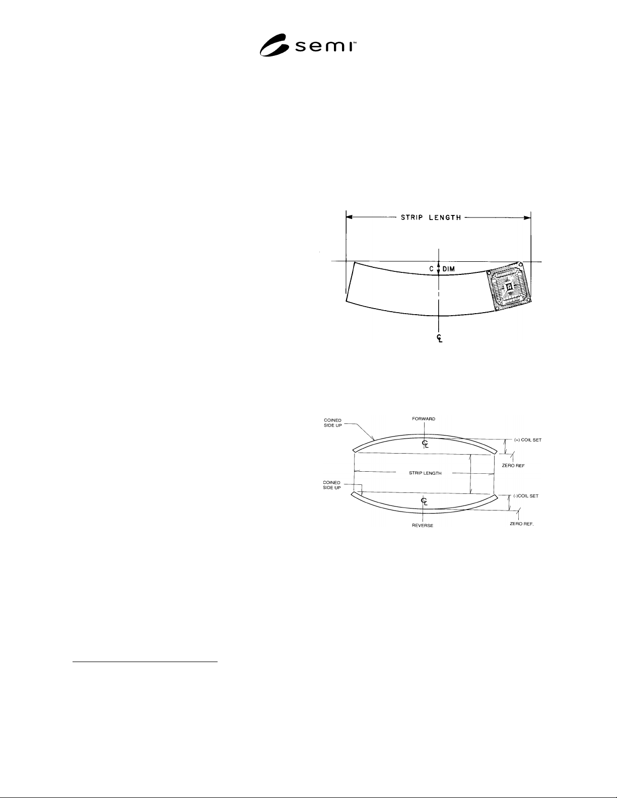
camber — curvature of the leadframe strip edge (see
Figure 1).
Figure 1
Camber
coil set — longitudinal bowing of the leadframe (see
Figure 2).
Figure 2
Coil Set
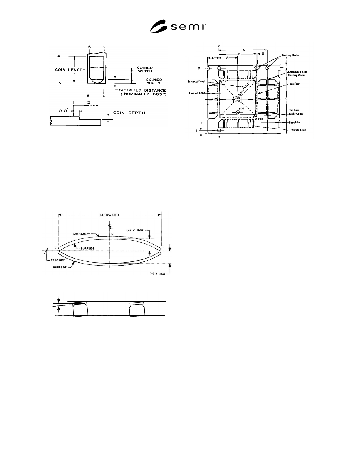
coined area — that area at the tip end of the bond
fingers coined to produce a flattened area for functional
use (see Figure 3).
SEMI G27-89 © SEMI 1985, 1989 2
Figure 3
Coined Area
crossbow — transverse bowing of the leadframe (see
Figure 4).
functional area — the die attach pad and the lead tips.
lead twist — angular rotation of bonding fingers (see
Figure 5).
pits — shallow surface depression or craters in the
leadframe material.
Figure 4
Crossbow
Figure 5
Lead Twist
slug marks — random dents in the leadframe caused by
foreign material in the stamping die.
stamped leadframe terminology — (See Figure 6.)
true position circle — the circle with its center
positioned at the center of the coined lead which
defines the design position of the lead tip.
Figure 6
Plastic Leaded Chip Carrier Leadframe
4 Ordering Information
4.1 Purchase orders for leadframes furnished to this
specification shall include the following information:
4.1.1 Current revision of the leadfra me drawing
detailing the base material and the plating type(s),
thickness(es) and area(s).
4.1.2 Reference to this specification.
4.1.3 Vendor certification requirements.
5 Dimensions
See Table 1.
6 Defect Limits and Parame ters
Note: Measurement methods are described in SEMI G10.
Alternate methods may be used as agreed to between vendor
and customer. The methods described in SEMI G10 are
considered to be standard for the purpose of solving
differences.
6.1 Dimensional Tolerances — Se e Figure 6.
6.2 Minimum Flat Wire Bonding Area — 80% of
nominal lead width and 0.635 mm (0.025") in length.
6.3 Coined Depth — 0.013 mm (0 .0005") min. to 30%
of material thickness maximum.
6.4 Horizontal Lead Spacing and Location (Lead
Tips)
SEMI G27-89 © SEMI 1985, 19893
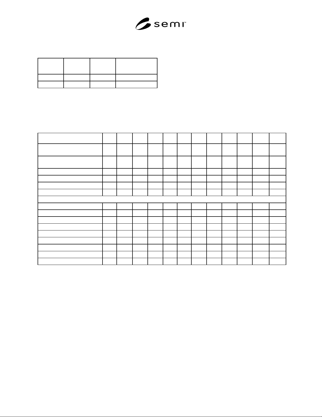
6.4.1 The lead spacing and lead loca tion that can be maintained is a function of the designed lead spacing and lead
width.
Design Lead
Width
Design Lead
Space
Minimum
Lead Sapce
Minimum True
Position Circle Dia.
≥ 0.011" ≥ 0.011" 0.006" 0.007"
0.010" 0.010" 0.005" 0.006"
Tolerances for lead designs smaller than .010" should be negotiated between vendor and user.
6.4.2 18 - 100 Pin Lead Frames — Leads to be located so that a 0.007" diameter circle centered on the nominal
center of the coined lead in width and 0.152 mm (0.006") back from lead tip in length shall be totally encompassed
by the coined area.
Table 1 Plastic Leaded Chip Carrier Leadframe Standard Dimensions (all dimensions in inches)
LEAD COUNT 18 LD 18 LD 20 LD 28 LD 28 LD 32 LD 44 LD 52 LD 68 LD 84 LD 100 LD 100 LD
PACKAGE SHAPE
Rect.
Rect.
Stretch Square Square Rect. Rect. Square Square Square Square Square Square
JEDEC
PACKAGEDESIGNATION
AA AB AA AB AD AE AC AD AE AF
Nominal Pkg. Width 0.290 0.290 0.350 0.450 0.350 0.450 0.650 0.750 0.950 1.150 1.350 1.150
Length 0.425 0.490 0.350 0.450 0.550 0.550 0.650 0.750 0.950 1.150 1.350 1.150
PROGRESSION 0.720 0.720 0.780 0.880 0.780 0.880 1.080 1.180 1.400 1.600 1.800 1.600
STRIP WIDTH 0.970 1.230 0.970 1.070 1.230 1.230 1.230 1.430 1.670 1.870 2.070 1.870
TOOLING DIMENSIONS (See Figure 6)
A 0.170 0.170 0.200 0.250 0.200 0.250 0.350 0.400 0.500 0.600 0.700 0.600
B 0.340 0.340 0.400 0.500 0.400 0.500 0.700 0.800 1.000 1.200 1.400 1.200
C 0.530 0.530 0.590 0.690 0.590 0.690 0.890 0.990 1.200 1.400 1.600 1.400
D 0.190 0.190 0.190 0.190 0.190 0.190 0.190 0.190 0.200 0.200 0.200 0.200
E 0.020 0.020 0.020 0.020 0.020 0.020 0.020 9.020 0.020 0.020 0.020 0.020
F 0.050 0.050 0.050 0.050 0.050 0.050 0.050 0.050 0.050 0.050 0.050 0.050
G 0.920 1.180 0.920 1.020 1.180 1.180 1.180 1.380 1.620 1.820 2.020 1.820
Diameter 0.060 0.060 0.060 0.060 0.060 0.060 0.060 0.060 0.060 0.060 0.060 0.060
Metal Thickness 0.010 0.010 0.010 0.010 0.010 0.010 0.010 0.010 0.008 0.008 0.008 0.008
Note 1: Gate — All packages; gate on the corner counter-clockwise from pin one.
Note 2: Dam Bar — Recommend 0.025 wide with 0.025 space between package and dam bar.
Note 3: Lead shall meet the JEDEC Quad Package requirements.
6.5 Horizontal Die Attach Pad Lo cation — Die attach pad shall be located within 0.051 mm (± 0.002") on 18-100
pin leads.
6.6 Lead Twist — Shall not exceed 3° 30' or 0.015 mm (0.0006") per 0.254 mm (0.010") of lead width.
6.7 Die Attach Pad Tilt and Flatness
6.7.1 Tilt — 0.025 mm (0.001") maximum per 2.54 mm (0.100") of length or width in the undepressed state. 0.051
mm (0.002") maximum per 2.54 mm (0.100") of length or width in the depressed conditions when measuring from
corner to corner.
6.7.2 Flatness — 0.005 mm (0.0002") per 0.100" pad length on 18-100 pin leadframes when measuring from the
center to the average of the four corners. The corners are defined at 0.127 mm (0.005") from each edge.
6.8 Die Attach Pad Downset or De pression — The nominal downset recommended is 0.015" (0.381 mm) ± 0.002".
6.9 Lead and Die Attach Pad Cop lanarity