semi合集-English.pdf - 第542页
SEMI E77-1104 © SEMI 1998, 2004 10 16.3 ISA St andard 3 ISA S51. 1 — Process Instrument ation Terminology 16.4 MIL-STD 4 MIL-STD 45662 — Calibration Systems Req uirements NOTICE: SEMI makes no warranties or represen tati…
SEMI E77-1104 © SEMI 1998, 2004 9
14.4 Interpretation
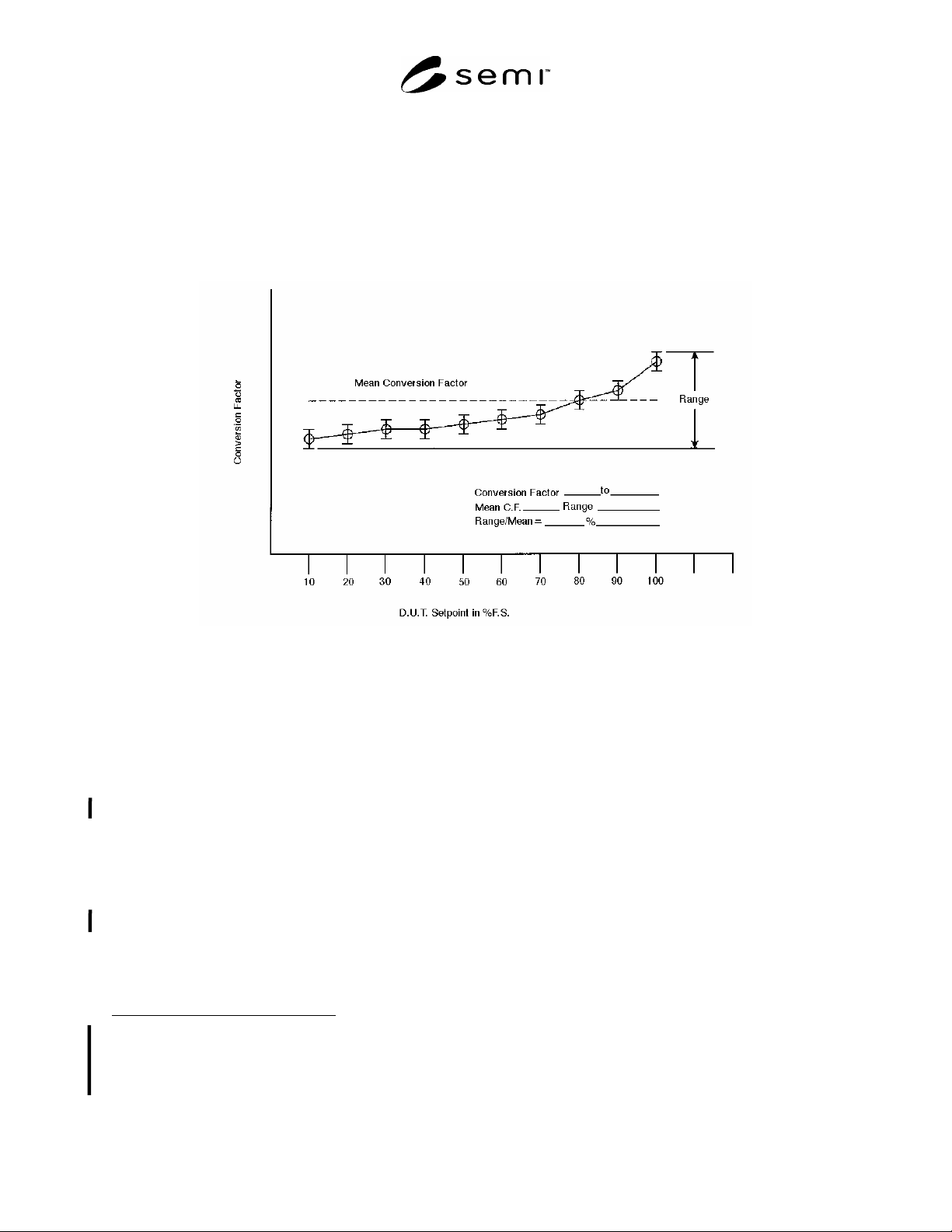
14.4.1 Figure 3 illustrates the conversion factor between two specific gases as a function of setpoint. It may be used
to accurately map from one gas to the other and may predict the flow error that will result if the average conversion
factor is used.
Nameplate Gas/Range ___________ Test Gas ________________ Date _____________
MFG/Serial # _________________ Barometric Pressure _______________
Inlet Pressure _________________ Temperature _____________________
Figure 3
Conversion Factors vs. D.U.T. Setpoint
15 Reporting Results
15.1 MFC Conversion Factors
15.1.1 Plot the conversion factor from Gas A to Gas B against the D.U.T. setpoint. Note the mean value and range
of values (see Figure 3).
16 Related Documents
16.1 ANSI Standards
1
ANSI C39.5 — Safety Requirements for Electrical and Electronic Measuring and Controlling Instrumentation
ANSI C42.100 — Dictionary of Electrical and Electronics Terms
ANSI MC4.1 — Dynamic Response Testing of Process Control Instrumentation
16.2 IEC Standard
2
IEC 546 — Methods of Evaluating the Performance of Controllers with Analogue Signals for Use in Industrial
Process Control
1 American National Standards Institute, Headquarters: 1819 L Street, NW, Washington, DC 20036, USA. Telephone: 202.293.8020; Fax:
202.293.9287, New York Office: 11 West 42nd Street, New York, NY 10036, USA. Telephone: 212.642.4900; Fax: 212.398.0023, Website:
www.ansi.org
2 International Electrotechnical Commission, 3, rue de Varembé, Case Postale 131, CH-1211 Geneva 20, Switzerland. Telephone:
41.22.919.02.11; Fax: 41.22.919.03.00, Website: www.iec.ch

SEMI E77-1104 © SEMI 1998, 2004 10
16.3 ISA Standard
3
ISA S51.1 — Process Instrumentation Terminology
16.4 MIL-STD
4
MIL-STD 45662 — Calibration Systems Requirements
NOTICE: SEMI makes no warranties or representations as to the suitability of the standards set forth herein for any
particular application. The determination of the suitability of the standard is solely the responsibility of the user.
Users are cautioned to refer to manufacturer's instructions, product labels, product data sheets, and other relevant
literature, respecting any materials or equipment mentioned herein. These standards are subject to change without
notice.
By publication of this standard, Semiconductor Equipment and Materials International (SEMI) takes no position
respecting the validity of any patent rights or copyrights asserted in connection with any items mentioned in this
standard. Users of this standard are expressly advised that determination of any such patent rights or copyrights, and
the risk of infringement of such rights are entirely their own responsibility.
3 Instrument Society of America, 67 Alexander Drive, Research Triangle Park, NC 27709, USA Telephone: 919.549.8411 Website: www.isa.org
4 United States Military Standards, Available through the Naval Publications and Forms Center, 5801 Tabor Avenue, Philadelphia, PA 19120-
5099, USA. Telephone: 215.697.3321
Copyright by SEMI® (Semiconductor Equipment and Materials
International), 3081 Zanker Road, San Jose, CA 95134. Reproduction
of the contents in whole or in part is forbidden without express written
consent of SEMI.

SEMI E78-1102 © SEMI 1998, 2002 1
SEMI E78-1102
ELECTROSTATIC COMPATIBILITY - GUIDE TO ASSESS AND
CONTROL ELECTROSTATIC DISCHARGE (ESD) AND
ELECTROSTATIC ATTRACTION (ESA) FOR EQUIPMENT
This guide was technically approved by the Global Metrics Committee and is the direct responsibility of the
North American Metrics Committee. Current edition approved by the North American Regional Standards
Committee on August 29, 2002. Initially available at www.semi.org September 2002; to be published
November 2002. Originally published September 1998.
1 Purpose
1.1 The purpose of this document is to minimize the
negative impact on productivity caused by static charge
in semiconductor manufacturing environments. It is a
guide for establishing electrostatic compatibility of
equipment used in semiconductor manufacturing.
1.2 Electrostatic surface charge causes a number of
undesirable effects in semiconductor manufacturing
environments. Electrostatic discharge (ESD) damages
both products and reticles. ESD events also cause
electromagnetic interference (EMI), resulting in
equipment malfunctions. Charged wafer and reticle
surfaces attract particles (electrostatic attraction or
ESA) and increase the defect rate. Charge on products
can also result in equipment malfunction or product
breakage. Operating problems and additional product
defects due to static charge can have a negative impact
on the cost of ownership of semiconductor
manufacturing equipment (refer to SEMI E35).
1.3 An increasing amount of semiconductor production
is done in minienvironments or within the production
equipment. The majority of static related problems
occur while the product is in its carriers, or being
transferred from them, by the production equipment.
1.4 Static control methods can be incorporated in the
equipment design to reduce static charge to acceptable
levels. This guide will be used primarily by equipment
manufacturers during the design of their equipment.
There are test methods available (see Sections 6 and 7
of this guide) to demonstrate the effectiveness of the
static control methods. The end user will be able to use
the same test methods to verify compliance with an
equipment purchase specification.
2 Scope
2.1 The scope of this document is limited to methods
of measurement and a guide for the maximum
recommended level of static charge on:
• Product or reticles,
• Carriers, and
• Parts of the input/exit ports of equipment and
minienvironments.
2.2 This document presents a matrix of maximum
recommended levels of static charge on products,
reticles, carriers, and the input and exit ports of
production equipment or minienvironments. The
purpose is to:
• Reduce product, reticle, and equipment damage
due to ESD,
• Reduce equipment lock-up problems due to ESD
events, and
• Reduce the attraction of particles to charged
surfaces.
2.3 This document references SEMI E43 and other
methods of measuring static charge. Related
Information 1 of this document contains a theoretical
investigation of electrostatic particle attraction, as well
as case histories from users and equipment
manufacturers as to the static charge problems
encountered and how they were solved. A bibliography
of related technical papers is also included. Related
Information 2 describes static control methods
commonly used in semiconductor manufacturing.
2.4 This standard does not purport to address safety
issues, if any, associated with its use. It is the
responsibility of the users of this standard to establish
appropriate safety health practices and determine the
applicability or regulatory limitations prior to use.
3 Limitations
3.1 Static Measurements — Measurements of
electrostatic quantities such as charge, electric field,
and voltage are difficult to make. The nature of the
object (insulator or conductor), its geometry, its
surroundings, and the measuring equipment itself, are
only a few of the factors affecting the accuracy of an
electrostatic measurement.
3.1.1 Similarly, it is difficult to relate the measurement
of an electrostatic quantity to its effect on products or
equipment. For example, an ESD simulator produces a
standardized discharge waveform when a capacitor is