semi合集-English.pdf - 第4203页
SEMI F73-1102 © SEMI 2002 5 17 Related Documents 17.1 ASTM Stan dards ASTM F1372-93 — Standard Test Method for Scanning El ectron Microscope (SEM) Analysis of Metallic Surface Condition for Gas Distribution System Comp o…

SEMI F73-1102 © SEMI 2002 4
collection efficiency. Any adhesives used to mount
samples must not contaminate the surface to be
analyzed. To remove loosely adhered surface particles,
the sample may be blown off immediately before
introduction into the SEM with clean, dry, 0.1
micrometer filtered gas.
14.2 Place the sample in the SEM chamber for
pumpdown. Activate the electron beam when vacuum
conditions meet manufacturer’s recommendations. The
instrument accelerating voltage should be a consistently
selected value within the range 15 to 25 Kev; 20 KeV is
suggested. The working distance should be within the
range recommended by the instrument manufacturer.
Sample position (tilt angle and orientation) may be
adjusted to optimize EDS detector collection efficiency
for EDS analysis.
14.3 Increase the magnification to ≥ 400× for initial
focus; adjust instrument parameters for astigmatism and
other anomalies. Decrease magnification to 200× and
move the sample while viewing until an area judged as
representative of the whole is in view. The area to be
analyzed should be as free of particles and defect
features produced by sample preparation as possible.
14.4 Refocus and record images of this area at 200×,
1000×, and a pre-selected, consistently used
magnification within the range 3000 to 3600×. Move
to another representative area and record an image at
the same 3000–3600× magnification. Move to a third
representative area and record another image at the
3000–3600× magnification.
14.5 Each area selected for recording should include a
defect or metallurgical feature to demonstrate proper
focusing, contrast adjustment and resolution capability.
Contrast adjustment should be performed per the
technique described in Section 4.7.2.1 of Scanning
Electron Microscopy and X-Ray Microanalysis.
5
All
defects and/or features for which the change in signal
∆S due to the contrast exceeds the noise N by a factor
of 5 minimum must be clearly distinguishable in the
image recorded (see Section 4.5 of reference 5).
14.6 If any inclusions or contamination are noted in the
3000–3600× images, EDS analysis of representative
defect(s) may be performed if requested by the
company for which the test method is performed.
Collect X-ray signals for a sufficient length of time to
obtain an integrated count of ≥ 250,000 within the
range of 0 to 10 keV.
5 Scanning Electron Microscopy and X-Ray Microanalysis: A Text
for Boilogists, Materials Scientists, and Geologists; Joseph I.
Goldstein, Dale E. Newbury, Patrick Echlin, David C. Joy, A. D.
Romig, Jr., Charles E. Lyman, Charles Fiori, Eric Lifshin; Second
Edition, Plenum Press, New York (1992).
15 Calculations or Interpretation of Results
15.1 The 3000–3600× recorded images shall be placed
under the transparent overlay grid. The number of grid
squares that contain all or part of a surface defect shall
be counted and summed for each photomicrograph.
Each such grid square shall only be counted once; it is
not the intent of this Test Method to count individual
defects. If a defect appears in more than one adjacent
grid square, each grid square occupied shall be counted.
NOTE 2: Examples of scanning electron micrographs
overlaid with an alphanumeric indexed grid showing specific
types of defects with comments on their locations and
whether they should be counted may be viewed at
http://www.semi.org/web/wstandards.nsf/url/SurfaceAnalysis
Examples.
15.2 Surface film residues resulting from improper
cleaning are generally diffuse and difficult to quantify.
These residues, if present, are counted as one per
image. Particles that loosely adhere to the surface must
be presumed to be artifacts of sample preparation or
exposure, and therefore shall be ignored.
15.3 Peaks appearing in the EDS spectra shall be
identified and the spectra labeled to indicate whether it
is a representative area, or identified as a defect from a
photomicrograph.
16 Reporting Results
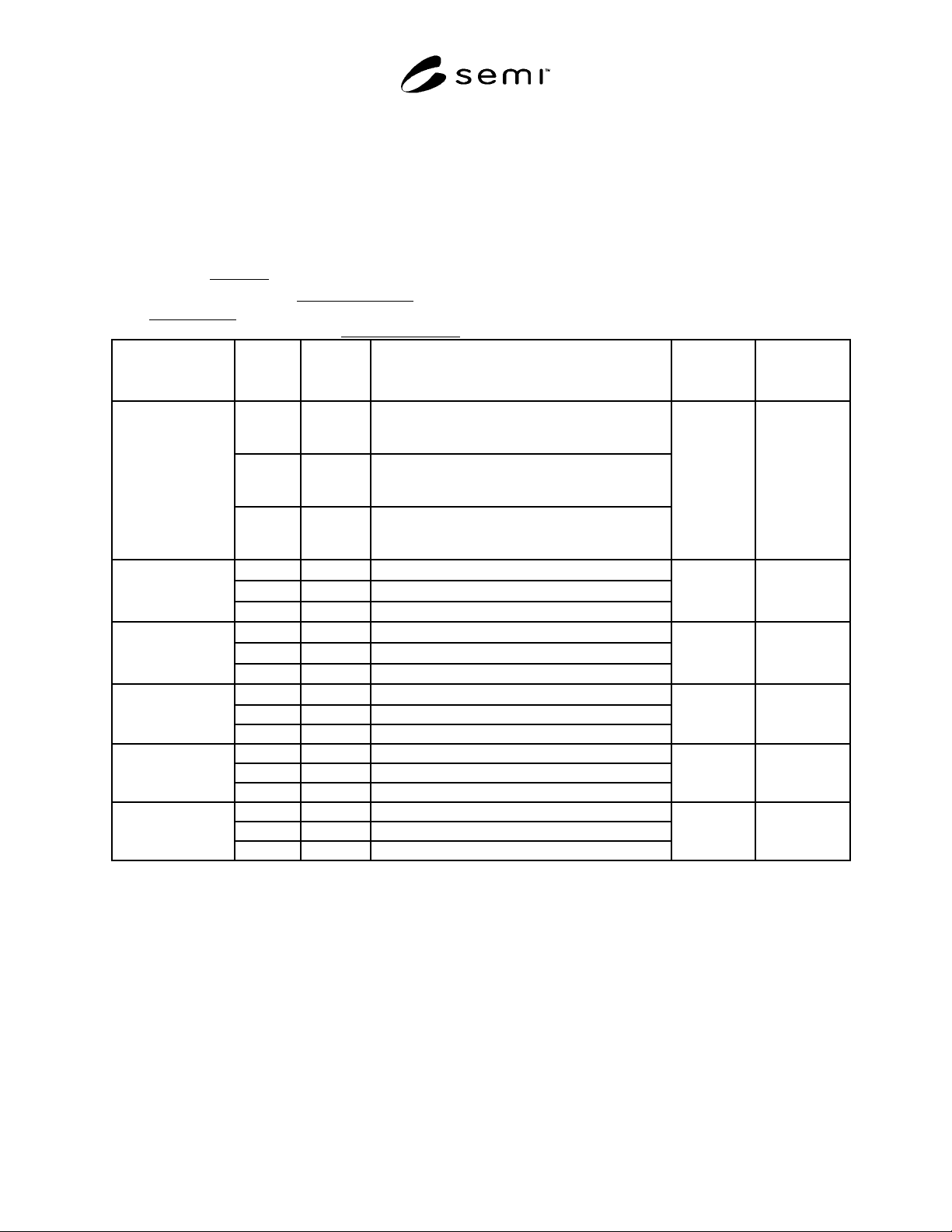
16.1 A tabular summary of defects counted per 3000–
3600× photomicrograph shall be presented.
Additionally, the table should indicate an average of
defect counts and the maximum from the three 3000–
3600× images. An example of a table reporting defect
counting results and the photomicrographs from which
the defect counts were taken are shown in Appendix 1.
16.2 All photomicrographs are to be permanently
labeled with sample identification, magnification, a
magnification scale bar, date, and analyst identification.
The photomicrographs should be available for
inspection upon request.
16.3 EDS spectra are to be labeled with the same
information, plus peak identifications. If any
instrument parameters (e.g., tilt angle) were changed for
EDS analysis, these must be noted. If peak height
differences are such that adequate representation of all
peaks cannot be made from the same plot, two plots
having different scaling shall be included.
Identification of each defect analyzed, either by arrow
on photomicrograph or by notation of grid position,
shall be made.

SEMI F73-1102 © SEMI 2002 5
17 Related Documents
17.1 ASTM Standards
ASTM F1372-93 — Standard Test Method for Scanning Electron Microscope (SEM) Analysis of Metallic Surface
Condition for Gas Distribution System Components
ASTM F1375-92 — Standard Test Method for Energy Dispersive X-Ray Spectrometer (EDX) Analysis of Metallic
Surface Condition for Gas Distribution System Components
SEMI F73-1102 © SEMI 2002 6
APPENDIX 1
EXAMPLE OF AN ACCEPTABLE FORMAT FOR REPORTING DEFECT
COUNTING RESULTS
NOTE: The material in this appendix is an official part of SEMI F73 and was approved by full letter ballot procedures.
Table A1-1 Example of an Acceptable Format for Reporting Defect Counting Results
Analyst Name: John Doe
Analytical Service Provider: ABC Services Lab
Date: May 10, 1999
(Customer; Order Number; Source): Pure Products, Inc.
Sample
Micro
No.
Defect
Count
Comments
(Location indexing optional)
Average
Count
Maximum
Count
1 (from
Figure
A1-1)
13 Inclusion J7, K7, I8, J8, K8; Pits A8, C7 and C8,
E9, F8, J9, I12, I15
2 (from
Figure
A1-2)
30 Stringer G14 to P3; Pit C13 and C14
A22-6/5/97
3 (from
Figure
A1-3)
4 Pits D10 and E10, G13. Grain, twin boundaries,
white sample prep debris not counted.
16
30
1 12 Pits; stringer
2 23 Scratch
(Sample #2
Identification)
3 16 Inclusion
17
23
1 9 Stringer
2 4
(Sample #3
Identification)
3 6 Pits
6
9