semi合集-English.pdf - 第6506页
SEMI G80-0200 © SE MI 2000 14 measurements are made they inclu d e these two parameters. Thus, becau se of the measurement if included per the definition, they would be double counted. 13.5 The OTA definition used in th …

SEMI G80-0200 © SEMI 200013
to establish Drive Input to Compare Output timing
error. Reference Figure 6.
12.2.6 As noted, Level 1 analysis does establish drive
input to compare output-timing error. But, Level 1
cannot independently determine and isolate drive input
timing error from compare output timing error, as was
accomplished in Level 2. What this means is if the
minimum to maximum drive input to compare output
timing error is established as 1ns (Level 1), the method
cannot create a break down such that so much of that
1ns is input error, with the remaining part of that 1ns
being the output error.
12.2.7 Table 2 data also contains other valuable
components of ATE error that will assist in establishing
ATE timing integrity. Tests that establish the various
components of Input Z Timing error, Multiple Period
Tests for on the fly timing, and for systems with a High
Speed Clock function tests to determine various delay,
jitter and time variation errors.
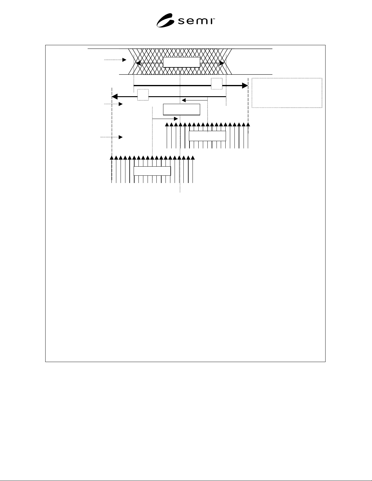
12.3 A brief word on Drive Input to Compare Output
Timing Accuracy will be made. Drive Input to
Compare Output Timing can be described in different
ways. It is easy to think of this parameter, per the
definition of this aspect of OTA (reference Figure 6), as
simply the relative time difference (skew) between
drive input delay timing (see SEMI G79) and compare
output delay timing (see SEMI G79), for a particular
machine.
16
But this parameter, once established, is not
necessarily constant. For example, this parameter can
change from one calibration of a machine at a particular
time, to something different, as a result of a subsequent
calibration of that same machine. As well, Drive Input
to Compare Output error can also be considered as a
machine to machine accuracy parameter, not
necessarily having the same value between any two
machines of the same kind.
12.3.1 Thus, on each machine and at different points
in time for the same machine the Drive Input to
Compare Output Timing skew can be uniquely different
per machine. That difference being influenced by the
various machine anomalies that contribute to machine
error including the not so perfect results of a periodic
edge calibration.
12.3.2 In the general case drive input to compare
output as shown in Figure 6 should be thought of in the
context of drive/compare edges having time variance
across multiple machines or as representing edges for
the same machine but having variance across multiple
time intervals associated with different calibrations.
16 Both drive input delay timing and compare output delay timing
values taken at center of spread. By definition center of spread is the
average of min & max: (minerr + maxerr)/2.
12.3.3 Examination of the OTA definition in the
context of Figure 6, that being the general case and not
a single point timing evaluation, reveals that the overall
timing accuracy time value is the time line indicated by
“A” and the time line indicated by “B”. In a single
point AC timing evaluation, OTA is determined as a
distribution of edges associated with time line “A” or
time line “B”, depending upon the relationship between
the drive edge values and compare edge values (see
SEMI G79) at that point in time.
13 Precision, Accuracy, and Precautions
13.1 Precision and Accuracy — Tolerances called-out
in the various steps of this procedure are consistent with
the required supplemental equipment specifications
called for in this Test Procedure.
13.2 Precautions — A precaution is advised when
executing this procedure to the letter. Unreliable
execution or failures may occur as a result of ATE
specification tradeoff that typically exists between
minimum pulse width and drive signal amplitude. This
can be especially true when operation is in conjunction
with complex formats such as SBC. This condition is a
result of specification limitations inherent in the system
under evaluation. Be advised that failure conditions
can occur for systems with inadequate minimum pulse
width and/or inadequate comparator bandwidth
characteristics operating this procedure at high
frequencies with complex formats.
13.3 It is necessary to note that data in Table 1 for any
particular test represents minimum and maximum
values taken for all conditions specified for each test.
Examples of these conditions are parameters such as
frequency, formats, and different voltages. Thus the
precaution lies in how the user interprets the minimum
to maximum deltas. As an example, a minimum value
can occur at a lower frequency whereas a maximum
value for that test may occur at a higher (different)
frequency. Be aware, deltas under broad conditions
may be greater than deltas for a focused condition.
This specification is defined to provide results for the
broad case.
13.4 When entering your analysis results to Table 2
Single Point Overall Timing Accuracy (OTA), be
advised that the Single Point OTA Result is represented
only as indicated in Table 2, the sum of Drive Input to
Compare Output Timing, Drive Input Timing Delay
Error, and Compare Output Time Delay Error. This
appears to deviate from the absolute definition of OTA
in that Drive Input Transition and Drive Input Timing
Cycle Jitter are not included. The method does not lend
itself to making Drive Input Timing Delay Error
measurements that exclude these two components. Per
this method when the Drive Input Timing Delay Error

SEMI G80-0200 © SEMI 2000 14
measurements are made they include these two
parameters. Thus, because of the measurement if
included per the definition, they would be double
counted.
13.5 The OTA definition used in this method does not
include reference parameters shown in Table 2 such as
Drive Input Z Timing Error, Extended Delay, Multiple
Period (timing on the fly), and High Speed Clock
measurements. These are strictly reference timing
parameters. This method is not defined such that they
are to be included as part of OTA. Thus the user is
advised not to sum any of those items as part of the
OTA value entered into Table 2.
13.6 Table 2 is labeled Single Point Overall Timing
Accuracy (OTA) Results. The term “single point” is
used as a reminder for the user of this document that
one execution of this method on a particular ATE
system does not in itself constitute an overall timing
accuracy conclusion for that system. It is simply a
sample of the ATE's performance at some point in time.
A true assessment of an ATE's performance for overall
timing accuracy requires a comprehensive analysis
involving data collection over an extended period of
time that goes well beyond what this method provides
in one pass.
13.7 In general, regarding these pre cautions, the user
is free to adjust the procedure and data collection
according to conditions consistent with the desired
objective. Regardless, if the procedure is performed
under anything other than full-up broad conditions, the
results must be identified as a subset or partial
interoperation of a single point overall timing accuracy
assessment.
14 Related Documents
None.
SEMI G80-0200 © SEMI 200015
For reference see the following definitions taken from SEMI G79:
7.1.1 Input Edge Placement Accuracy — DUT input timing error comprised of input timing delay error, input timing jitter and
input transition time variation.
7.1.2 Output Edge Placement Accuracy — DUT output compare timing error comprised of output timing delay error and
output compare timing jitter.
Output Timing Delay Error –– time delay error at the detected midpoint of a 5V transition, with respect to an ideal delay
(NIST traceable reference), using any pin, any delay value, any compare timing edge,
window or strobe compare mode, expect H or L, positive or negative transition and any test
cycle length.
Conditions:
- measured with load circuit “off” or high impedance
- delays normalized to rising edge detected by pin 1, using strobe compare format, expect H, @ 0ns
- error normalized to the average of min & max of the error distribution
- input signal: 50-ohm source, 0–5V step, > 1V/ns, inserted at a zero length interconnect on the
DUT side of a standard performance board
Output Compare Timing Jitter –– short term (cycle to cycle) instability using any pin, any compare timing edge, window or
strobe compare mode, expect H or L. (NOTE: This document does not define a method
for Output Compare Timing Jitter.)
Conditions:
- error expressed as RMS value
- physical reference point is a zero length interconnect on the DUT side of a standard performance board
- jitter referenced to an independent synchronous trigger
7.1.3 Input to Output Timing Accuracy — relative time difference between the input delay timing and
output delay timing.
See SEMI G79.
Drive Input Edge Placement
Accuracy (See SEMI G79.)
(Verification = Sections
10.4.1, 10.4.3, and 10.4.4)
See SEMI G79.
B
A
Drive Input to Compare
Output Timing Accuracy
(See SEMI G79.)
(Verification – Section
10.3.1)
Compare Output Edge
Placement Accuracy (See
SEMI G79) (Verification –
Section 10.4.2, NOTE: This
does not include compare
j
itter.)
Overall Timing Accuracy
(+A, -B)
(Verification = Sections
10.4.1, 10.4.2, and 10.3.1)
Output timing delay
error.
See SEMI G79.
Output Delay Timing Error –– For another
machine, or a new spread for the same machine
as a result of a calibration.
See SEMI G79.
Figure 6
Overall Timing Accuracy (OTA)