semi合集-English.pdf - 第261页
SEMI E43-0301 © SEMI 1995 , 2001 9 items susceptible to discharges equal to or greater than 100 V HBM. ESD SP10.1 — A utomated Handl ing Equi pment. This document covers t est meth ods for evaluating t he ESD ground inte…
SEMI E43-0301 © SEMI 1995, 2001 8
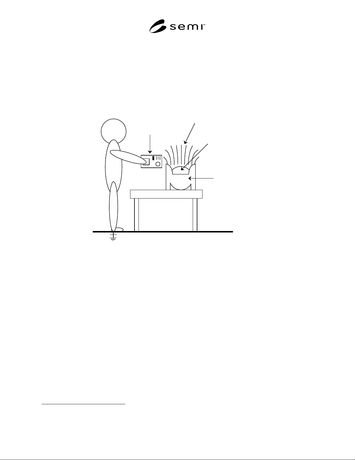
A) Make sure meter is properly grounded according to manufacturer's
instructions.
B) Scan approximately 2.54 cm along both sides and ends of carrier.
C) Scan approximately 2.54 cm length of carrier and top-center of
wafers with meter.
D) Note high-low values for B) & C).
E) Assure that the operator is properly grounded.
Meter
Field emanating from carrier of charge
semiconductor wafers.
Wafers
Ground Plane
Carrier
Figure 4
Example of a Survey of a Carrier of Semiconductor Wafers
12 Related Documents
NOTE 2: These documents are for information only; in the
case of conflict, this document takes precedence. Also read/be
aware of appendices to this document before use.
12.1 ESD Association Standards
1
ANSI EOS/ESD S3.1: Ionization. Test methods and
procedures for evaluating and selecting air-ionization
equipment and systems are provided in this standard,
which establishes measurement techniques to determine
ion balance and charge-neutralization time for ionizers.
ESD STM4.2: Worksurfaces — Charge Dissipation
Characteristics. This standard test method prescribes a
procedure for measuring the electrostatic-charge-
dissipation characteristics or work surfaces used for
ESD control.
1 ESD Association, 7900 Turin Rd., Bldg. 3, Suite 2, Rome, NY
13440-2069, website: www.esda.org
ESD STM5.1: ESD Sensitivity Testing — Human Body
Model. This standard test methods defines procedures
for testing, evaluating, and classifying the ESD
sensitivity of components to the defined Human Body
Model (HBM).
ESD S5.2: ESD Sensitivity Testing — Machine Model.
This standard established a test procedure for
evaluating the ESD sensitivity of components to a
defined Machine Model, and outlines a system whereby
the sensitivity of such components may be classified.
ESD STM5.3.1: ESD Sensitivity Testing — Charged
Device Model. This standard is a test method for
evaluating active and passive components’ ESD
sensitivity to a defined Charged Device Model.
ANSI/ESD S20.20: ESD Control Program. This
standard specifies the requirements that must be
satisfied in designing, establishing, implementing, and
maintaining ESD control programs for ESD-sensitive

SEMI E43-0301 © SEMI 1995, 20019
items susceptible to discharges equal to or greater than
100 V HBM.
ESD SP10.1 — Automated Handling Equipment. This
document covers test methods for evaluating the ESD
ground integrity of automated handling equipment as
well as charge generation, and charge accumulation on
devices in automated handling equipment.
12.2 ESD Association Advisory Documents
ESD ADV1.0 — Glossary of Terms. Definitions and
explanations of various terms used in Association
Standards and documents are covered in this advisory.
It also includes other terms commonly used in the ESD
industry.
ESD ADV2.0 — ESD Handbook. The ESD Handbook is
a complete guide to static control in the work place.
Nineteen chapters cover ESD basics, control
procedures, auditing, symbols, device testing, and
standards.
ESD ADV11.2 — Triboelectric Charge Accumulation
Testing. The complex phenomenon of triboelectric
charging is discussed in this Advisory. It covers the
theory and effects of tribocharging. It reviews
procedures and problems associated with various test
methods that are often used to evaluate
triboelectrification characteristics.
12.3 Other Related Documents
12.3.1 Military Standards
2
MIL-STD-1686C: ESD Control Program for Protection
of Electrical and Electronic Parts, Assemblies and
Equipment (Excluding Electrically Initiated Devices).
This military standard establishes requirements for ESD
control programs. It applies to U.S. military agencies,
contractors, subcontractors, suppliers, and vendors. It
requires the establishment, implementation, and
documentation of ESD control programs for static-
sensitive devices but does not mandate or preclude the
use of any specific ESD control materials, products, or
procedures.
MIL-HDBK-263B: ESD Control Handbook for
Protection of Electrical and Electronic Parts,
Assemblies and Equipment (excluding Electrically
Initiated Explosive Devices). This reference provides
guidance, but not mandatory requirements, for the
establishment and implementation of an ESD control
program in accordance with the requirements of MIL-
STD-1686.
2 Naval Publication and Forms Center, 5801 Tabor Avenue,
Philadelphia PA 19120 U.S.A
12.3.2 JEDEC Standards
3
JESD625A: Requirements for Handling ESD-Sensitive
Devices. This voluntary standard establishes minimum
requirements for ESD control methods and materials
designed to protect electronic devices having Human
Body Model (HBM) sensitivities of 200 V or greater. It
is intended for use by semiconductor distributors,
semiconductor processing and testing facilities, and
semiconductor end users.
12.3.3 EIA Standards
4
EIA 541 – Packaging Material Standards for ESD
Sensitive Items — This standard presents requirements
and tests methods for selecting packaging materials to
be used with ESD sensitive devices.
EIA 583 – Packaging Material Standards for Moisture
Sensitive Items — This standard contains information
regarding packaging materials used for the protection of
ESD sensitive items when moisture levels are also
important.
EN100015: Protection of Electrostatic Sensitive. This
European Norm covers ESD handling practices for
electronic devices.
12.3.4 IEC Standards
5
IEC 61000-4-2 – Transient Immunity Standard. This
IEC document provides requirements and test methods
for ESD transient immunity.
IEC 61340-5-1:1998, Electrostatics, Part 5-1:
Protection of Electronic Devices from Electrostatic
Phenomena-General Requirements. This IEC
(International Electrotechnical Commission) document
provides guidance for establishing a static control
program.
IEC 61340-5-2:1999, Protection of Electronic Devices
from Electrostatic Phenomena-Users Guide. This IEC
handbook supplement the information contained in Part
5-1 above.
3 Joint Electron Device Engineering Council, 2500 Wilson Blvd.,
Arlington, VA 22201, website: www.jedec.org
4 EIA Engineering Department, Standards Sales Office, 2001 Eye
Street, NW, Washington, D.C. 20006, website: www.eia.org
5 International Electrotechnical Commission, 3, rue de Varembé,
Case postale 131, CH-1211 Genève 20, Switzerland, website:
www.iec.ch
SEMI E43-0301 © SEMI 1995, 2001 10
APPENDIX 1
MEASUREMENT SELECTION MATRIX
NOTE: This appendix offers information related to selecting the appropriate measurement methods from those contained in this
document. It was approved as an official part of SEMI E43 by full letter ballot procedure.
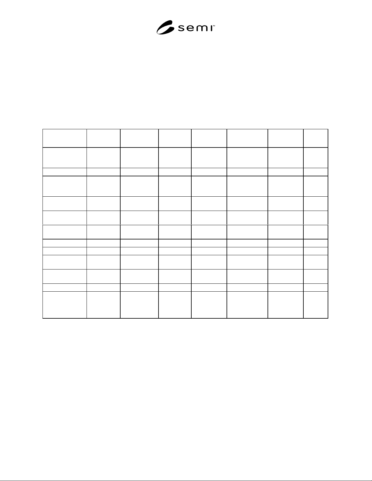
A1-1 The matrix contained in Table A1-1 is intended to assist in the selection of an appropriate measurement
method for static charge. Users should note that a variety of measurement methods is available for any given
situation. Consult manufacturers of the equipment for additional information concerning its proper use and
applicability.
Table A1-1 Measurement Method Recommendations
Object Electrostatic
Fieldmeter
Charged Plate
Monitor
Electrostatic
Voltmeter
Electrometer Coulombmeter Oscilloscope EMI
Detector
Small
object/device
charge
XX X
Surface charge X X
Ionization system
charge
neutralization
XXX
ESD event
detection
XXX
Human body
voltage
XXX
Product cart
charge level
XXX
Chair charge level X X X
Charge decay X X X X
Product material
handling
XXX
Ionizer Offset
Voltage (Balance)
XX
Wafer charge X X X
Process
equipment –
Charge and ESD
generation
XXX X
NOTICE: SEMI makes no warranties or representations as to the suitability of the standards set forth herein for any
particular application. The determination of the suitability of the standard is solely the responsibility of the user.
Users are cautioned to refer to manufacture's instructions, product labels, product data sheets, and other relevant
literature, respecting any materials or equipment mentioned herein. These standards are subject to change without
notice.
By publications of this standard, Semiconductor Equipment and Materials International (SEMI) takes no position
respecting the validity of any patent rights or copyrights asserted in connection with any items mentioned in this
standard. Users of this standard are expressly advised that determination of any such patent rights or copyrights, and
the risk of infringement of such rights are entirely their own responsibility.