semi合集-English.pdf - 第5826页
SEMI P28-96 © SEM I 1996 2 physi cal con ditions (e.g., ph otoresist islan d on met al over an oxide window). The u ser should fu rt her st ate which features constitute the su b strate geometry and which constitute the …

SEMI P28-96 © SEMI 19961
SEMI P28-96
SPECIFICATION FOR OVERLAY-METROLOGY TEST PATTERNS FOR
INTEGRATED-CIRCUIT MANUFACTURE
1 Purpose
1.1 This document defines several standard overlay-
metrology patterns that are used by metrology
equipment users to evaluate and test micropatterning
equipment and processes in integrated circuit (IC)
manufacturing. These overlay cells may be placed by
optional patterning methods onto substrates during the
manufacturing process. Usage of the standard overlay
patterns is an attempt to provide consistent
industrywide use of automated metrology equipment.
2 Scope
2.1 This specification defines general designs that
describe the shape, size, design rules, and placement
considerations (where appropriate) of several basic
patterns for overlay metrology. These standard test
patterns can be used for optical, scanning electron
beam, and other types of metrology.
3 Limitations
3.1 The patterns described in this document represent
the first pass at an industrywide commonality for the
purpose of compatibility among various types of
automated metrology equipment. It is not suggested,
however, that these test patterns are a full complement
or are optimal for all overlay-metrology applications.
This document does not attempt to specify how the
patterns are to be imaged or measured on the substrate.
4 Referenced Documents
4.1 SEMI Documents
SEMI International Standards Handbook — Section E:
Compilation of Terms
SEMI P6 — Specification for Registration Marks for
Photomasks
SEMI P18 — Specification for Overlay Capabilities of
Wafer Steppers
SEMI P19 — Specification for Metrology Pattern Cells
for Integrated Circuit Manufacture
4.2 ASTM Standard
1
F 127-84 — Definition of Terms Relating to
Photomasking Technology for Microelectronics
1 American Society for Testing and Materials, 100 Barr Harbor
Drive, West Conshohoken, PA 19428-2959
5 Terminology
5.1 centerline — a reference line that is equidistant
from opposite edges of a feature.
5.2 feature — areas within a singl e continuous
boundary (for example, an aggregate image) that have
any physical property that is distinct from the
background area outside the feature (e.g., the simplest
element of a test pattern, such as a single line or bar).
Some physical properties that may distinguish the
feature are the refractive index, surface roughness, etc.
5.3 feature dimension — the dime nsion of interest;
such as, the side of a box , bar width, and/or length.
5.4 overlay (micropatterning)
A vector quantity defined at every point on the wafer.
It is the difference,
O , between the vector position, 1P ,
of a substrate geometry, and the vector position of the
corresponding point, 2P , in an overlaying pattern,
which may consist of photoresist. [SEMI P18-92]
NOTE: All overlay test patterns are designed to provide
both X and Y components of the vector overlay.
5.5
pattern, overlay test — a grou p of features for
overlay metrology.
5.6
pitch — the distance between a point on an image
and the corresponding point on the corresponding
image in an adjacent functional pattern.
5.7
substrate (materials) — in semiconductor
technology, a wafer that is the basis for subsequent
processing operations in the fabrication of
semiconductor devices or circuits. [ASTM F 1241-89]
NOTE: The meaning of substrate is not limited to
wafers.
6 General Specification
6.1 Introduction
6.1.1 This specification describes th e overlay test
patterns that are illustrated in the figures at the end of
this document. The imaging means by which these test
patterns are defined on the substrate may be selected by
the user (see 6.2.1).
6.1.2
Characteristics of the overlay patterns, such as
materials, topography, polarity, and method of pattern
transfer will be defined by the user unless otherwise
noted. When reporting measurements extracted from
these overlay test patterns, the user should state the

SEMI P28-96 © SEMI 1996 2
physical conditions (e.g., photoresist island on metal
over an oxide window). The user should further state
which features constitute the substrate geometry and
which constitute the overlaying pattern (terms as used
in the definition of overlay in 5.4). In general, the
vectors P1 and P2 terminate at the geometrical centers
of the substrate pattern and the overlaying pattern
respectively.
6.2
Applications
6.2.1 The overlay test patterns are intended to be used
in a variety of applications. The following applications
list shows some uses for the overlay test patterns.
• Primary Pattern Generation
• Lithography & Metrology Equipment
Characterization
• In-Line Process Overlay Monitoring
• Manufacturing Characterization
• Process Transfer Between Manufacturing Sites
6.3 Guidelines
6.3.1 The overlay test patterns descr ibed herein
represent a basic metrology set from which composite
patterns may be constructed.
6.3.2
Each overlay test pattern has a fundamental
design. The user may adjust the dimensions
appropriately as they apply to the user’s specific
processing/equipment situations.
6.3.3
It is required that labels, borde r lines, indicator
marks, or any other adjacent features be avoided, or at
least separated by a minimum of ten (10) micrometers
from the overlay cell. This proximity guideline is
defined to remind the user that patterns intended to be
independent and symmetric be designed as
circumstances permit. The user should determine actual
spacing values, because spacing may be level-, process-
, and/or tool-dependent.
6.3.4
It is recognized that there are design limitations
dictated by the equipment and processes used to
generate the pattern (e.g., computer aided graphics
(CAD) grids, pattern generation (PG) rectangles, E-
beam spot sizes). The user may modify the overlay test
patterns in order to meet equipment limitations (e.g.,
stay on grid) provided that the resulting patterns or their
representations retain the designed structures and
symmetry.
7 Detailed Specification
7.1 Introduction
7.1.1 The figures provided within th is document are
intended to illustrate sample layouts of several overlay
test patterns, and to define appropriate design elements
used within each. The overlay test pattern dimensions
are provided when appropriate. It is understood that, to
optimize the test pattern’s performance in a specific
application, the user may deviate beyond this standard.
7.2
Specific Overlay Patterns — A ll patterns have 90°
rotational symmetry.
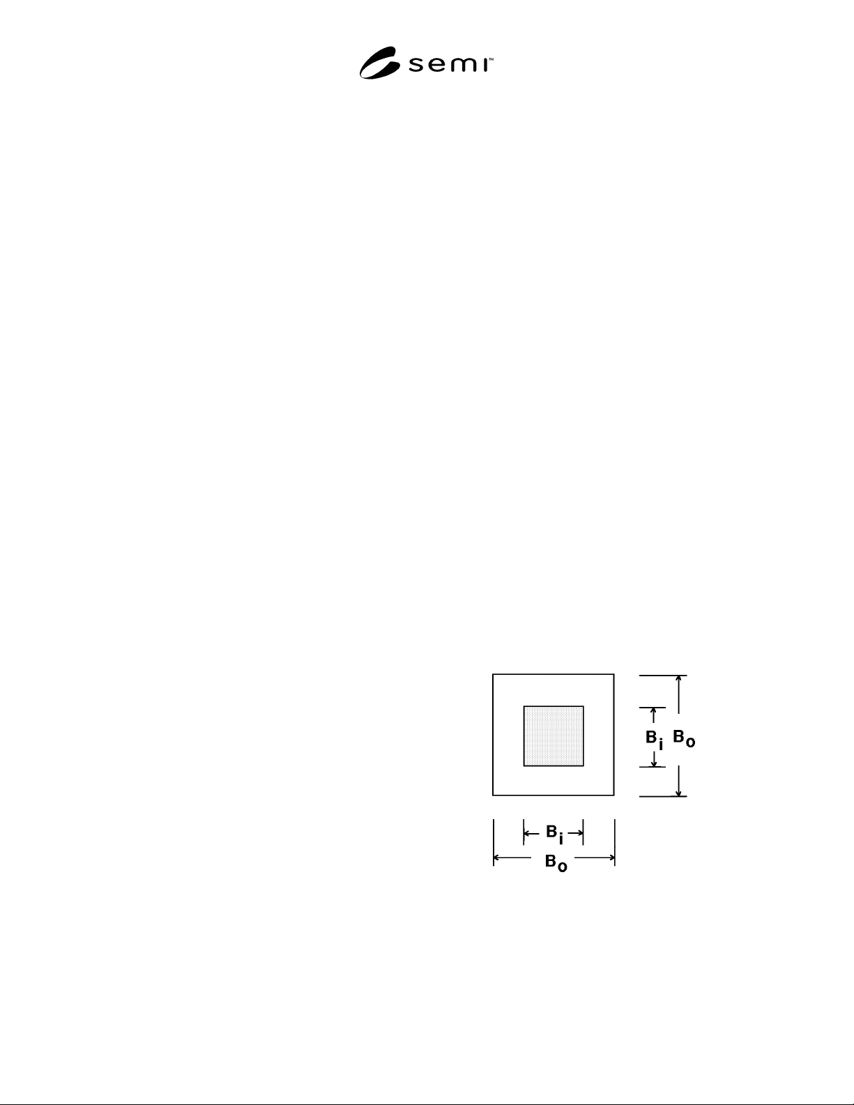
7.2.1 Box-in-Box (see Figure 1)
7.2.1.1 The box-in-box test pattern is designed to be a
test pattern for overlay measurement on metrology
equipment. This is the simplest possible design
presented.
7.2.1.2
The box-in-box test pattern consists of two
square features. Each box is normally defined by a
different imaging step; that is, one box corresponds to
the substrate geometry and the other box corresponds to
the overlaying pattern (5.4). The two boxes are
designed to be concentric.
7.2.1.3
The design elements are the feature dimensions
of the outer box, B
o
, and of the inner box, B
i
. The
dimensions should follow these guidelines:
outer box: B
o
= 12 – 30 micrometers (µm)
inner box: B
i
= B
o
/2
These specifications define a range of box sizes and
their interfeature spacing. Users should modify the box-
in-box dimensions as dictated by design rules, process,
and/or measurement equipment requirements. The user
should recognize that edges in close proximity may
cause measurement errors.
7.2.2
Frame-in-Frame (see Figure 2)
7.2.2.1 The frame-in-frame test patter n is designed to
be a test pattern for overlay measurement on metrology
equipment. It has two designed edges per axis on each
side of each imaged step. The additional information
gained by having two features on each level, each with
a centerline, may reduce the measurement uncertainty
as compared to the box-in-box design.
7.2.2.2
The design elements are the pi tch of opposite
members of the outer frame (F
o
), the pitch of opposite
members of the inner frame (F
i
), and the widths of the
frames (W
o
and/or W
i
) as shown in Figure 2. Each
frame is normally defined by a different imaging step;
that is, one frame corresponds to the substrate geometry
and the other box corresponds to the overlaying pattern
(see 5.4). The frames are designed to be concentric.
7.2.2.3
The design elements are the outermost
dimension of the outer frame (F
o
), the outermost
SEMI P28-96 © SEMI 19963
dimension for the inner frame (F
i
), and the width(s) of
the frames (W
o
and/or W
i
). The dimensions should
follow these guidelines:
outer frame: F
o
= 15–30 micrometers (µm)
inner frame: F
i
= F
o
/2
width: W = 1.0–1.5 µm for F
o
≤ 24 µm, or 1.5–2.0
µm for F
o
≥ 24 µm
NOTE: The width of the inner and outer bars may differ.
These specifications define a range of frame sizes and
their interfeature spacing. Users may modify the frame-
in-frame dimensions as dictated by design rules,
process, and/or measurement equipment requirements.
7.2.3
Bars-in-Bars (see Figure 3)
7.2.3.1 The bars-in-bars test pattern is designed to be a
test pattern for overlay measurement on metrology
equipment. Each axis has two designed edges per axis
on each side of each imaging step. The additional
information gained by having two features on each
level, each with a centerline, may reduce the
measurement uncertainty as compared to the box-in-
box design.
7.2.3.2
The overlay test pattern consists of two sets of
bars, the outer set and the inner set. Each set of bars is
arranged to form an overlay measurement frame as
shown in Figure 3. Each bar-in-bar set is normally
defined by a different imaging step; that is, the set of
inner bars corresponds to the substrate geometry and
the set of outer bars corresponds to the overlaying
pattern (5.4), or vice versa. The two sets of bars are
designed to be concentric.
7.2.3.3
The design elements are the pi tch for the outer
set of bars (B
o
), the pitch for the inner set of bars (B
i
),
the length of the outer bars (L
o
), the length of the inner
bars (L
i
), and the width(s) of the bars (W
o
and/or W
i
).
The overlay test pattern dimensions should follow these
guidelines:
outer bar set: B
o
= 15–30 µm
inner bar set: B
i
= B
o
/2
outer bar length: L
o
= 50%–70% B
o
inner bar length: L
I
= 50%–70% B
i
width: W = 1.0–1.5 µm for B
o
≤ 24 µm, or 1.5–2.0
µm for B
o
≥ 24 µm
NOTE: The width of the inner and outer bars may differ.
These specifications define a range of box sizes and
their interfeature spacing. Users may modify the box-
in-box dimensions as dictated by design rules, process,
and/or measurement equipment requirements. The user
should recognize that edges in close proximity may
cause measurement errors.
7.3
User Considerations for Overlay-Metrology
Equipment
7.3.1 Pattern Acquisition — To ensure automatic
acquisition of the desired overlay test pattern by an
image-based automated overlay metrology equipment,
one or more of the following may be required:
1. Separation of each overlay test pattern as required
per metrology equipment specification.
2. Use of only one overlay test pattern in the
measurement field-of-view.
3. Printing unique labels next to each overlay test
pattern using the proximity guideline in Section
6.3.3.
7.3.2
Feature Dimensions — For each overlay test
pattern, only a range of feature dimensions is defined
(e.g., paragraph 7.2.2.3). The user and supplier together
should determine that the dimensions of the overlay test
patterns they select are those that consider design rules,
the user’s process capability, and limitations of the
microlithography and measurement equipment.
7.3.2.1
Width Dimensions (frame-in-frame or bars-in-
bars test patterns) — When all features of the overlay
test pattern are imaged at the same process step, the
widths of the inner and outer features are recommended
to be equal, and of the same polarity, in order to
minimize overlay-measurement errors.
Figure 1
Box-in-Box