semi合集-English.pdf - 第7697页
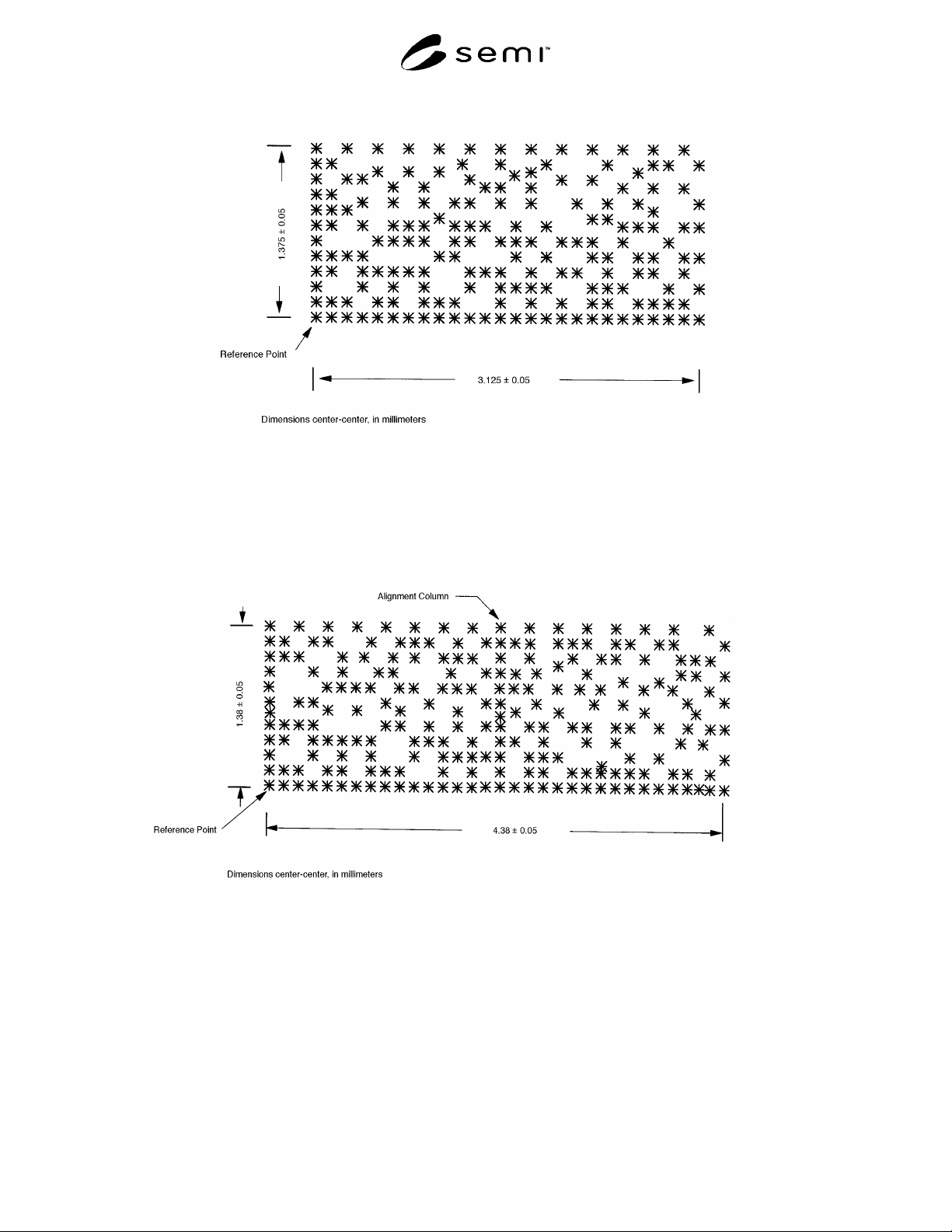
SEMI T8-0698 E © SEMI 1998, 2004 6 Figure 5 Data Matrix Code Field Figure 6 Data Matrix Code Field
SEMI T8-0698
E
© SEMI 1998, 2004 5
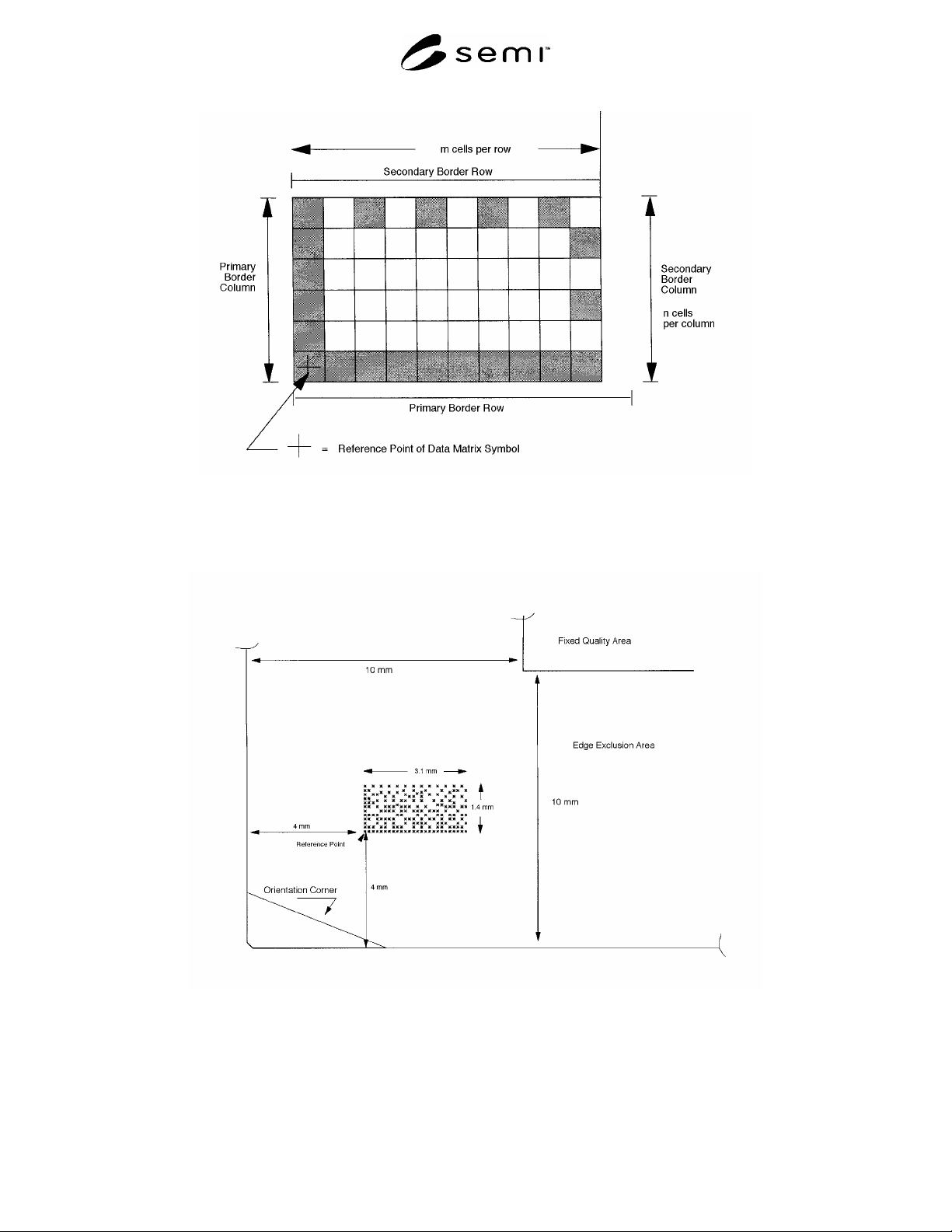
Figure 3
Border Rows and Columns
Figure 4|
Data Matrix Code Field in Edge Exclusion Area
SEMI T8-0698
E
© SEMI 1998, 2004 6
Figure 5
Data Matrix Code Field
Figure 6
Data Matrix Code Field
SEMI T8-0698
E
© SEMI 1998, 2004 7
APPENDIX 1
PLACEMENT OF DATA MATRIX CODES ON DISPLAY SECTIONS OF
FLAT PANEL DISPLAY SUBSTRATES
NOTICE: This appendix was approved as an official part of SEMI T8, but the recommendations in this appendix
are optional and are not required to conform to this standard.
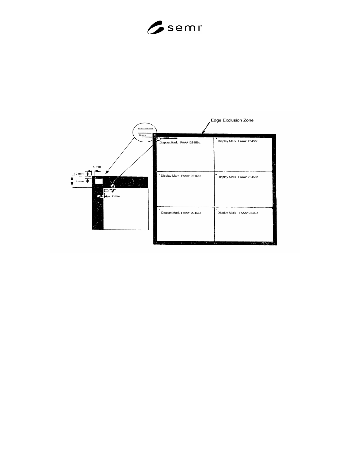
A1-1 The following suggests one way in which individual display sections could be marked while still a part of the
motherglass substrate. Figure A1-1 illustrates a six-up display layout on a 550 × 650 mm substrate
Figure A1-1
An Example of Mark Field Locations in Individual Display
Sections within a “Motherglass” Substrate
A1-2 The Substrate ID location falls within the edge exclusion area as detailed in Figure 4. In this example, all ID
fields are located on the back (non-pattern) surface. Placing them on the same surface as the substrate mark can
simplify ID reading during fabrication. Their location on the non-pattern surface could allow ID reading of the
outside surface of a display after assembly.
A1-3 The axes of the individual display IDs are parallel to the substrate ID axes. Each display ID is located adjacent
to a display corner. The locations of each ID field are given.
NOTE A1-1: This example does not constitute a recommended usage, but is intended to assist users in developing ID locations
suitable for their operations.