semi合集-English.pdf - 第6502页
SEMI G80-0200 © SE MI 2000 10 10.4.5.1 Thi s can be don e by making p e r io d measure- ments of the high speed clock ch a nnel un der test, wi t h a high bandwidth, digital sa mpling oscilloscope . A 50- ohm probe s hou…

SEMI G80-0200 © SEMI 20009
interaction using a generic measurement method. The
signal measurement should be made with the driver
loaded with reference load A (500 ohms in parallel with
2.5pF ± 0.5pF of capacitance). The following nested
loop outline describes the test flow:
for amplitude = 1V, 3V, 5V (optional)
for pin = 1 to n
for edge = rising to falling
measure the 20% to 80% transition time of a
NR driver signal with test cycle = 10*min,
delay = 0s using oscilloscope (averaging = 8)
error = maximum transition time - minimum
transition time
end edge
end pin
end amplitude
10.4.3.2 The transition time measurements are to be
made between the measured 20% and 80% points of
both positive and negative signal edges, i.e., the 20%
and 80% points on the signal transition edge relative to
a 0% or 100% steady state level displayed on the
oscilloscope. Ideally, measurement points chosen
should be referenced to a steady state level that results
after all aberrations in the transition have expired. Use
the lowest tester pin as a reference channel when setting
the measurement points for these measurements.
10.4.3.3 ATE systems may use a focused calibration
routine for driver pins. That routine is intended to
correct edge error due to transition time variations. In
the context of executing this method for a machine that
has this capability, the user of this method is advised to:
1) Execute the Drive Input Transition Time Variation
test regardless, and 2) Enter the test results to the
method data summary, Table 2. The entry in Table 2
for transition variation will be a reference parameter.
This method as defined is incapable of making drive
edge error measurements that exclude transition
variation and jitter.
10.4.4 Driver Input Timing Cycle Jitter Test
12
—
Since driver input timing jitter cannot be determined
from Level 1 tests, an external instrument must be used
to measure short term, cycle to cycle (or period)
instability. This can be done by making period
measurements of the driver-input channel under test,
with a high bandwidth, digital sampling oscilloscope.
A 50-ohm probe should be used to minimize
measurement jitter. The tolerance for this test is ±
12 Trigger off the scope probe for this and the subsequent jitter test. Use
a high persistence display to show signal jitter. Use of a high bandwidth-
sampling oscilloscope with statistical capability is recommended.
Instrumentation jitter should be extracted from the measured signal jitter,
as explained in Appendix 4.
20ps
13
(min-max) due to the tester/instrument
interaction using a generic measurement method. The
measurement results are expressed as RMS. This
measurement depends on the jitter distribution being
Gaussian. Reference Appendix 4 for additional detail
regarding this measurement. If in the application of this
method it is determined that the jitter is non-Gaussian,
skip this test and make the appropriate notation on the
exceptions page (Appendix 3).
10.4.4.1 The following nested loop outline describes
the test flow:
for pin = 1 to n
for amplitude = 3V
for test_cycle = 2*min
for format = RTZ
for format_delay = 50%
for pulse_width = 50%
for i = 1 to 1000
meas(i) = measure the period of the pin under test
end i
measured signal jitter = RMS spread of meas(1)
through meas(1000)
end pulse_width
end format_delay
end format
end test_cycle
end amplitude
end pin
measured instrumentation jitter = RMS spread of
oscilloscope trigger
(method described further in Appendix 4)
actual RMS signal jitter = measured signal jitter -
measured instrumentation jitter
(via sum of squares - reference Appendix 4)
Reference load B (50 ohms to ground) should be used
for this measurement.
10.4.5 High Speed Clock Self-trigger Cycle Jitter Test
— If the ATE is configured with dedicated high speed
clock pins, an external instrument must be used to
measure short term, cycle to cycle (or period)
instability.
13 When recording measurement data, log all measurements as they are
taken from the measurement equipment and show the associated
equipment tolerances as a separate entity.
SEMI G80-0200 © SEMI 2000 10
10.4.5.1 This can be done by making period measure-
ments of the high speed clock channel under test, with a
high bandwidth, digital sampling oscilloscope. A 50-
ohm probe should be used to minimize measurement
jitter. The tolerance for this test is ± 20ps
(min-max)
due to the tester/instrument interaction using a generic
measurement method. The measurement results are
expressed as RMS. This measurement depends on the
jitter distribution being Gaussian. Reference Appendix
4 for additional detail regarding this measurement. If in
the application of this method it is determined that the
jitter is non-Gaussian, skip this test and make the
appropriate notation on the exceptions page (Appendix
3). The following nested loop outline describes the test
flow:
for pin = (all high speed clock pins)
for amplitude = 3V
for test_cycle = 10*min to min by min
for clock_delay = 50%
for i = 1 to 1000
meas(i) = measure the period of the clock pin under
test
end i
measured signal jitter = RMS spread of meas(1)
through meas(1000)
end format_delay
end test_cycle
end amplitude
end pin
measured instrumentation jitter = RMS spread of
oscilloscope trigger
(method described further in Appendix 4)
actual RMS signal jitter = measured signal jitter -
measured instrumentation jitter
(via sum of squares - reference Appendix 4)
Reference load B (50 ohms to ground) should be used
for this measurement.
Trigger
Edge
Measure
Jitter
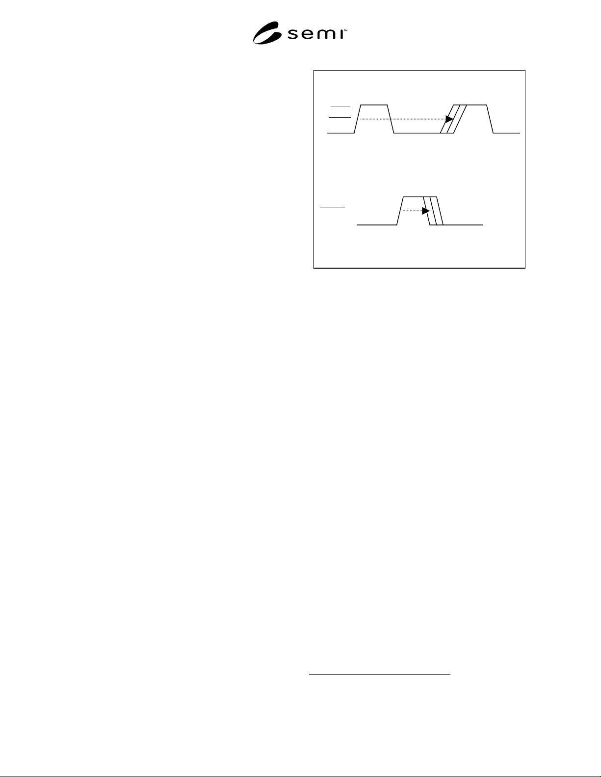
10.4.4
& 10.4.5
Cycle Jitter
Trigger
Edge
Measure
Jitter
10.4.6
Phase (PW) Jitter
Figure 5
Jitter Tests – Sections 10.4.4, 10.4.5 and 10.4.6
10.4.6 High Speed Clock Self-trigger Phase Jitter Test
— If the ATE is configured with dedicated high speed
clock pins, an external instrument must be used to
measure short term, phase (or duty cycle) instability.
This can be done by making pulse width measurements
of the high speed clock channel under test, using a high
bandwidth, digital-sampling oscilloscope. A 50-ohm
probe should be used to minimize measurement jitter.
The tolerance for this test is ± 20ps
14
(min-max) due to
the tester/instrument interaction using a generic
measurement method. The results are expressed as
RMS.
10.4.6.1 This measurement depends on the jitter
distribution being Gaussian. Reference Appendix 4 for
additional detail regarding this measurement. If in the
application of this method it is determined that the jitter
is non-Gaussian, skip this test and make the appropriate
notation on the exceptions page (Appendix 3). The
following nested loop outline describes the test flow:
for pin = (all high speed clock pins)
for amplitude = 3V
for test_cycle = 10*min to min by min
for clock_delay = 50%
for i = 1 to 1000
meas(i) = measure the pulse width of the clock pin
under test
end i
measured signal jitter = RMS spread of meas(1)
through meas(1000)
end format_delay
14 When recording measurement data, log all measurements as they are taken
from the measurement equipment and show the associated equipment tolerance
as a separate entity.

SEMI G80-0200 © SEMI 200011
end test_cycle
end amplitude
end pin
measured instrumentation jitter = RMS spread of
oscilloscope trigger
(method described further in Appendix 4)
actual RMS signal jitter = measured signal jitter -
measured instrumentation jitter
(via sum of squares - reference Appendix 4)
Reference load B (50 ohms to ground) should be used
for this measurement.
11 Data Collection Tables
11.1 Table 1 is the data collection table. Data can be
manually or automatically entered to this table as this
procedure is executed, depending upon how the user
chooses to implement data collection.
11.2 Table 2 is intended to contain the final
conclusions or analysis results of this procedure. Data
for this table is taken from Table 1. Instructions for
entering data to Table 2 will be described in Section 12,
Reporting and Interpretation of Results, of this
procedure. Examples of OTA calculations and data
entry to Table 2 are contained in Appendix 2.
NOTE 4: A blank version of Table 2 is contained in Appendix
1.
12 Reporting and Interpretation of Results
12.1 Reporting Results — A large amount of data will
be gathered when this Test Method is executed per the
requirements of this method. A subset of this data
should be collected into Table 1. This table contains the
minimum and maximum values for the various tests
contained in this Test Method.
12.1.1 Table 2 is a summary revealing the results of
this Test Method. Table 2 entries will be determined
from values taken out of Table 1 as well as summations
of various entries occurring in Table 2. The following
is a guide to making entries to Table 2:
12.1.2 Driver Input Timing Delay Error (Section
10.4.1) — This value is taken from Table 1. It is the
difference between the minimum and maximum values
shown in Table 1 for this parameter.
12.1.3 Driver Input Timing Cycle Jitter (Section
10.4.4) — This value is taken from Table 1. This is the
RMS values shown in Table 1 for this parameter.
12.1.4 Driver Input Transition Time Variation
(Section 10.4.3) — This value is taken from Table 1. It
is the difference between the minimum and maximum
values shown in Table 1 for this parameter.
12.1.5 Driver Input Edge Placement Accuracy —
Driver Input Edge Placement by definition is the
summation of Driver Input Timing Delay Error
(Section 10.4.1), Driver Input Timing Cycle Jitter
(Section 10.4.4), and Driver Input Transition Time
Variation (Section 10.4.3). Regardless, since Drive
Input Timing Delay Error measurements defined in this
method do not exclude edge transition variation and
jitter this entry is simply the measurements results
obtained for Drive Input Timing Delay Error Level 2
(Section 10.4.1). Enter this value into Table 2 as Driver
Input Edge Placement.
12.1.6 Compare Output Time Delay Error (Section
10.4.2) — This value is taken from Table 1. It is the
difference between the minimum and maximum values
shown in Table 1 for this parameter.
12.1.7 Compare Output Edge Placement Accuracy —
Compare Output Edge Placement will be entered into
Table 2 as the same entry made for Compare Output
Time Delay Error (Section 10.4.2).
12.1.8 Drive Input to Compare Output Timing
Accuracy — Data taken from Table 1 for Section 10.3.1
results: Drive Input To Compare Output Timing
Accuracy = Reference – [(Min Value + Max Value)/2].
Refer to examples in Appendix 2.
12.1.9 Overall Timing Accuracy (OTA) — By
definition and in the general case, the OTA value is the
sum of Driver Input Edge Placement Accuracy,
Compare Output Edge Placement Accuracy, and Driver
Input to Compare Output Timing Accuracy. Examples
are provided in Appendix 2 for making this entry into
Table 2.
NOTE 5: For all High Speed Clock parameters shown in
Table 2: High Speed Clock Delay and High Speed Clock
Transition are parameters that use the same procedures as
Drive Input Timing Delay and Drive Input Transition Time
Variation. High Speed Clock Delay and High Speed Clock
Transition are parameters provided in this procedure to
accommodate those systems that have different pin
electronics for the High Speed Clock function. If the system
under evaluation doesn't have a High Speed Clock function,
then the steps in this procedure for all High Speed Clock
Accuracy are not required. High Speed Clock Cycle Jitter
and High Speed Clock Phase Jitter are reference parameters
with their respective test provided in this procedure to reveal
accuracy for the High Speed Clock function when that
function is present.
12.1.10 High Speed Clock Delay Error (Section
10.4.1) — This value is taken from Table 1. It is the
difference between the minimum and maximum values
shown in Table 1 for this parameter.
12.1.11 High Speed Clock Cycle Jitter (Section 10.4.5)
— This value is taken from Table 1. This is the RMS
values shown in Table 1 for this parameter.