semi合集-English.pdf - 第5486页
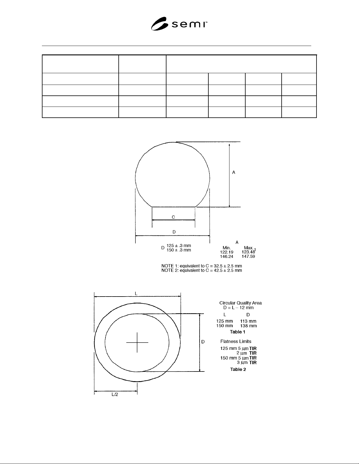
SEMI P4-92 © SEMI 1983, 1999 3 Table 1. Dimensions for Ro und Quartz Photomask Substrates PLATE SIZE ROUNDNESS (T. B. A. L ater D ate) PLATE THICKNESS Dimension (D) Dimension Tolerance Min. Tolerance Max. Units 125 Diame…
SEMI P4-92 © SEMI 1983, 1999 2
6.3 Physical Properties Information on the
following properties is provided for information only.
(See Appendix 1.)
6.3.1 Poisson' s Ratio
6.3.2 Density
6.3.3 Young' s Modulus
6.3.4 Modulus of Elasticity
6.3.5 Index of Refraction
6.3.6 Volume Restivity
7. Flatness Area (for one side only)
7.1 Flatness Quality Area
7.1.1 Circular Flatness Quality Area (See Tables 2
and 5.)
8. Visual Criteria (one side only)
8.1 Quality Area (See Tables 2 and 5.)
Plate Diameter Quality Area (Diameter)
125 mm 113 mm
150 mm 138 mm
8.2 Defect Limits Defects and allowable number of
each type are listed in Table 4.
8.2.1 Terminology for SEMI P4 Unless otherwise
noted, the SEMI Terms and Definitions Relating to the
Microlithography Industry shall be used.
8.2.2 Minimal Conditions or Dimensions Mini-mal
conditions or dimensions for defects are listed in Table
4 and shall be used for determining substrate
acceptability unless other minimal limiters are agreed
upon by the interested parties.
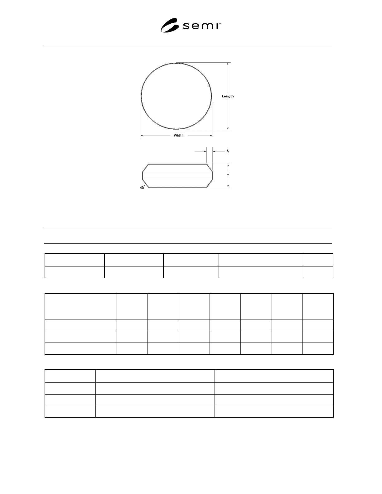
8.2.3 Photomask Substrate Edge Criteria (See
Table 3.)
8.3 Identification To be agreed upon between the
user and supplier.
9. Sampling
Unless otherwise specified, ASTM E 122 shall be used.
When so specified, appropriate samples sizes shall be
selected from each lot in accordance with MIL-STD-
105D. Each quality characteristic shall be assigned an
acceptable quality level (AQL) and lot total percent
defective (LTPD) value in accordance with MIL-STD-
105D. Definitions for critical, major and minor
classifications may alternatively be assigned cumulative
AQL and LTPD values. Inspection levels shall be
agreed upon between the user and supplier.
10. Test Methods
10.1 Thermal Expansion Determine in accordance
with ASTM E 228.
10.2 Transmission (To be agreed upon between the
user and supplier).
10.3 Flatness (To be agreed upon between the user
and supplier).
10.4 Visual (To be agreed upon between the user
and supplier.)
10.5 Roundness 2 readings at 90° with appropriate
tool such as Vernier Caliper or equivalent. Roundness
values not specified at this time.
11. Handling
Substrates are to be handled on the edges only.
Substrates are to be handled only with clean room
approved gloves.
12. Certification
Upon request of the purchaser in the contract or order, a
manufacturer' s or supplier' s certification that the
material was manufactured and tested in accordance
with this specification together with a report of the test
results shall be furnished at the time of shipment.
13. Packing and Marking
13.1 Substrates shall be packed in a class 100
environment as defined by ISO 14644-1. Containers
shall be designed to prevent glass-to-glass contact and
to protect the substrates from contamination in handling
and transit. Substrates shall be shipped with the
acceptable flatness side toward the front of the box.
This orientation shall be indicated on each container.
Packaging shall comply with the applicable
international, national, state, and local laws and
regulations required for shipping.
13.2 Containers shall be labeled " Warning: Open and
Handle Under Clean Room Conditions Only." Each
shipment shall be identified by user purchase order
number, drawing number (if applicable), quantity,
vendor lot number and material identification.
SEMI P4-92 © SEMI 1983, 1999 3
Table 1. Dimensions for Round Quartz Photomask Substrates
PLATE SIZE
ROUNDNESS
(T. B. A. Later Date)
PLATE THICKNESS
Dimension (D) Dimension Tolerance Min. Tolerance Max. Units
125 Diameter 125 ± .3
2.3 2.17 2.43 mm
150 Diameter 150 ± .3
2.3 2.17 2.43 mm
3.0 2.87 3.13 mm
SEMI P4-92 © SEMI 1983, 1999 4
Table 2. Flatness Limits for Round Quartz Photomask Substrates
Table 3. Edge Criteria for Round Quartz Photomask Substrates
Table 4. Glass Substrate Defect Limits per Plate
Internal Defects in the Quality Area
OPAQUE SPOT BUBBLE TOTAL DEFECTS (per inch
2
) NOTES
ULTE Glass
≥ 2 µm ≥ 2 µm
0.05 1 & 2
Surface Defects in the Quality Area
RESIDUE
SCRATCH
SIZE
TOTAL
DEFECTS
SLEEK SIZE
TOTAL
DEFECTS
(per in.
2
)
OPAQUE
SPOT SIZE
TOTAL
DEFECTS
(per in.
2
)
FRONTSIDE ULTE Glass
None
≥ 1.0 mm
0
≥ 2 µm
0
≥ 2.0 µm
0
< 1.0 µm
No limit
1-2 µm
0.1
1-2.0 µm
0.1
BACKSIDE ULTE Glass
≥ 3.0 µm
None
≥ 3.0 µm
None
≥ 10 µm
0.3
Defects Outside the Quality Area
EDGE CHIPS Defect Limit Total Number
Radial Depth
≥ .030"
None
Peripheral Cord
≥ .030"
None
Other Shall be negotiated between vendor and supplier. Shall be negotiated between vendor and supplier.
NOTES:
1. The size of internal defects is defined as 1/2 (long axis + short axis).
2. This table is based on the assumption that defects < 2 µm will fall outside the focal depth of the lens system and should not print.
T
A
2.3 mm (.090") .10 mm (min.) - .6 mm (max.)
3.0 mm (.120") .10 mm (min.) - .6 mm (max.)
Chamfered Edge Criteria