semi合集-English.pdf - 第7540页
SEMI MF1809-0704 © SEMI 2003, 2004 5 Table 3 Classification of Appli cation and Issue Suitability for Ch romium Free Etching S o lutions Application Issue Solution Name 100 Orientation 111 Orientation p-Type P+ Type n- T…
SEMI MF1809-0704 © SEMI 2003, 2004 4
8.3.1.3 Maintain 1 L of solution for each 1,000 cm
2
of
sample surface area to control temperature effects.
8.3.1.4 Etch the specimen according to the removal and
agitation restriction provided in the selection tables.
The time of the etching process may be derived by use
of the suggested etching depth for specific defects.
NOTE 4: Suggested removals may be found in SEMI
MF1725 and SEMI MF1726.
8.3.1.5 If the etching solution must be contained at the
point of use, decant the solution into a container for
(hazardous) waste and rinse the specimen thoroughly
with running water. If the solution is chromium-free
and is not contained for disposal, the solution may be
quenched with water and thoroughly rinsed in the same
beaker.
8.3.1.6 Blow the specimen dry with filtered, organic
free nitrogen.
8.3.1.7 Store the specimen in a clean container until
inspected.
9 Related Documents
9.1 Additional information may be found in the
following references that report details of various
etching solutions:
Sirtl, E., and Adler, A. “Chromic Acid-Hydrofluoric
Acid as Specific Reagents for the Development of
Etching Pits in Silicon,” Z. Metalkunde, 52, 529 (1961).
Secco d’Arragona, F., “Dislocation Etch for (100)
Planes in Silicon,” J. Electrochem. Soc., 110, 948,
(1972).
Schimmel, D.G., “Defect Etch for <100> Silicon
Evaluation,” J. Electrochem. Soc., 126, 479 (1979).
Wright-Jenkins, M., “A New Preferential Etch For
Defects in Silicon Crystals,” J. Electrochem. Soc., 124,
757, (1977).
Yang, K.H., “ An Etch for the Delineation of Defects in
Silicon,” J. Electrochem. Soc., 131, 1140 (1984).
Dash, W.C., “Copper Precipitation on Dislocations in
Silicon,” J. Appl. Phys., 27, 1193 (1956).
Chandler, T.C., “MEMC Etch-A Chromium Trioxide-
free Etchant for Delineating Dislocation and Slip in
Silicon,” J. Electrochem. Soc., 137, 944 (1990).
Sopori, B.L., “A New Defect Etch for Polycrystalline
Silicon,” J. Electrochem. Soc., 131, 667 (1984).
10 Keywords
10.1 defect density; dislocation; grain boundary;
microscopic; polycrystalline imperfection; preferential
etch; silicon; slip
Table 1 Recipes, Figure Index, and Approximate Etch Rates for Chromium Free Etching Solutions
Solution Name See Figures Recipe Approximate Etch Rate
Copper-3
1−2
(with agitation)
HF : HNO
3
: HAc : H
2
O : Cu(NO
3
)
2
·3H
2
O
@
36 : 25 : 18 : 21 : 1 g/100 ml total volume
1 µm/min
Copper-3
3−8
(without agitation)
HF : HNO
3
: HAc : H
2
O : Cu(NO
3
)
2
·3H
2
O
@
36 : 25 : 18 : 21 : 1 g/100 ml total volume
5 µm/min
Modified Dash 9-16
HF : HNO
3
: HAc : H
2
O
@
1 : 3 : 12: 0.17 + AgNO
3
0.005 to 0.05 g/L
1 µm/min
Table 2 Recipes, Figure Index, and Approximate Etch Rates for Chromium Containing Etching Solutions
Solution Name See Figures Recipe Approximate Etch Rate
Secco
17−22
HF : K
2
Cr
2
O
7
(0.15 M)
@
2 : 1
1 µm/min
Wright
23−32
HF : HNO
3
: CrO
3
(5 M) : HAc : H
2
O : Cu(NO
3
)
2
·3H
2
O
@
2 : 1 : 1 : 2 : 2 : 2 g/240 ml total volume
0.6 µm/min
SEMI MF1809-0704 © SEMI 2003, 2004 5
Table 3 Classification of Application and Issue Suitability for Chromium Free Etching Solutions
Application Issue
Solution Name
100 Orientation
111 Orientation
p-Type
P+ Type
n- Type
n+ Type
OISF
Shallow Pits
Hillocks
Dislocations
Epi Stacking
Faults
Bubble Formation
Agitation Required
Temperature
Flow Patterns
Copper-3 with Agitation A A A D A D A A C A A Yes Yes ~ 25° C No
Copper-3 without Agitation A A A D A D A A C A A Yes No ~ 25° C No
Modified Dash A A A C A D A A - A A Yes Yes ~ 25° C No
NOTE1: Classifications in Tables 3 and 4 are as follows: A = Excellent, B= Good, C= Acceptable, D = Unacceptable.
Table 4 Classification of Application and Issue Suitability for Chromium Containing Etching Solutions
Application Issue
Solution Name
100 Orientation
111 Orientation
p-Type
P+ Type
n- Type
n+ Type
OISF
Shallow Pits
Hillocks
Dislocations
Epi Stacking
Faults
Bubble Formation
Agitation Required
Temperature
Flow Patterns
Secco (NOTE 2) A B A D A C A B C A A Yes Yes < 30° C No
Wright A A A B A C A B B A A Yes Yes < 30° C No
NOTE 1: Classifications in Tables 3 and 4 are as follows: A = Excellent, B= Good, C= Acceptable, D = Unacceptable.
NOTE 2: Flow pattern defects form a characteristic “ v” shaped pattern when the wafer is etched in a vertical position without acid agitation (see
Figure 19). Other applications of Secco etch require some form of agitation to avoid confusing artifacts associated with bubble formation.
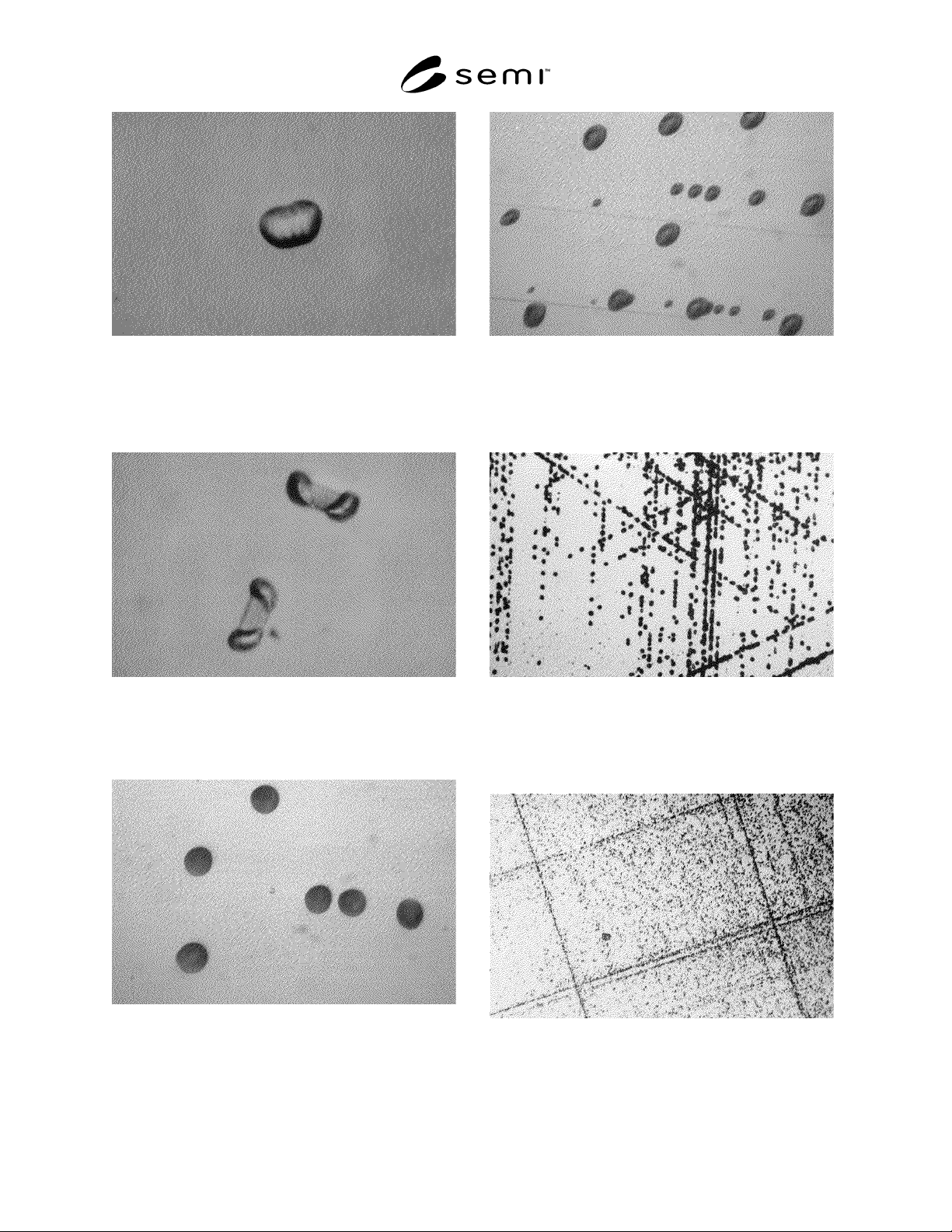
type, 10 Ω·cm, (100) Wafer; 1100° C Steam, 80 minute
Oxidation; Copper-3 Etch with Agitation; 2 µm removal
Figure 1
Oxidation Stacking Fault, 500
×
p type, 10 Ω·cm, (111) Wafer; 1100° C Steam, 80 minute
Oxidation; Copper-3 Etch with Agitation; 2 µm removal
Figure 2
Shallow Pits (Haze), 500
×
SEMI MF1809-0704 © SEMI 2003, 2004 6
p type, 10 Ω·cm, (100) Wafer; 1100° C Steam, 80 minute
Oxidation; Copper-3 Etch without Agitation; 1 µm removal
Figure 3
Oxidation Stacking Fault, 1000
×
p type, 10 Ω·cm, (100) Wafer; 1100° C Steam, 80 minute
Oxidation; Copper-3 Etch without Agitation; 1 µm removal
Figure 4
Oxidation Stacking Fault, 1000
×
p type, 10 Ω·cm, (111) Wafer; Copper-3 Etch without
Agitation; 10 µm removal
Figure 5
Dislocations, 500
×
p type, 10 Ω·cm, (100) Wafer; Copper-3 Etch without
Agitation; 10 µm removal
Figure 6
Dislocations, 500
×
p type, 10 Ω·cm, (111) Wafer; Copper-3 Etch without
Agitation; 10 µm removal
Figure 7
Slip Dislocations, 500
×
p type, 10 Ω·cm, (100) Wafer; Copper-3 Etch without
Agitation; 10 µm removal
Figure 8
Slip Dislocations, 100
×