semi合集-English.pdf - 第6216页
SEMI G43-87 © SEMI 198 6, 1987 4 R Θ JR = T J − T R P H(Package) junction - to - reference point where R Θ JR = R Θ JA and T R =T A . 6 Summary Report The following details shall be specified as appropr iate: a. Descript…

SEMI G43-87 © SEMI 1986, 19873
emitter-base voltage of bipolar transistors. Other
appropriate temperature-sensitive parameters may be
used for indirectly measuring junction temperature for
fabrication technologies that do not lend themselves to
sensing the active junction voltages.
5.2.2.1 Steady-State Technique for Measuring T
J
—
The following symbols shall apply for the purpose of
these measurements:
I
M
— ring current in milliamperes.
V
MH
— Value of temperature-sensitive parameters in
millivolts, measured at I
M
, and corresponding to the
temperature of the junction heated by P
H
.
T
MC
— Calibration temperature in degrees Celsius,
measured at the reference point.
V
MC
— Value of temperature-sensitive parameter in
millivolts, measured at I
M
and specific value of T
MC
.
The measurement of T
J
using junction forward voltage
as the TSP is made in the following manner:
Step 1 — Measurement of the temperature coefficient
of the TSP (calibration).
The coefficient of the temperature-sensitive parameter
is generated by measuring the TSP as a function of the
reference point temperature, for a specified constant
measuring current, I
M
, by externally heating the device
under test in an oven or in a fluid bath. The reference
point temperature range used during calibration shall
encompass the temperature range encountered in the
power application test (see Step 2). The measuring
current is generally chosen such that the TSP decreases
linearly with increasing temperature over the range of
interest and that negligible internal heating occurs in the
silicon and metal traces. For determining the optimum
TSP calibration or measuring current, V
MC
vs. log I
M
curves for two temperature levels that encompass the
calibration temperature range of interest should be
plotted. The optimum measuring current, I
M
, is then
selected such that it resides on the linear portion of the
two V
MC
vs. log I
M
curves that were generated. A
measuring current ranging from 0.05 to 5 mA is
generally used, depending on the specifications and
operating conditions of the device under test, for
measuring the TSP. The value of the TSP temperature
coefficient V
MC
/T
MC
, for the particular measuring
current used in the test, is calculated from the
calibration curve, V
MC
vs. T
MC
. At least three points
should be used to generate the voltage vs. temperature
curve for the determination of the TSP temperature
coefficient.
Step 2 — Power application test.
The power application test is performed in two parts.
For both portions of the test, the reference point
temperature is held constant at a preset value. The first
measurement to be made is that of the temperature-
sensitive parameter, i.e., V
MC
, under operating
conditions with the measuring current, I
M
, used during
the calibration procedure. The microelectronic device
under test shall then be operated with heating power
(P
H
) applied. The temperature-sensitive parameter,
V
MH
, shall be measured with constant measuring
current, I
M
, that was applied during the calibration
procedure (see Step 1).
The heating power, P
H
, shall be chosen such that the
calculated junction-to-reference point temperature
difference as measured at V
MH
is ≥ 20°C. In
accomplishing this, the device under test should not be
operated at such a high heating power level that the on-
chip temperature-sensing and heating circuitry is no
longer electrically isolated. Care should also be taken
not to exceed the design ratings of the package-
interconnect system, as this may lead to an
overestimation of the power being dissipated in the
active area of the chip due to excessive power losses in
the package leads and wire bonds. The values of V
MH
,
V
MC
, and P
H
are recorded during the power application
test.
The following data shall be recorded for these test
conditions:
a. Temperature-sensitive electrical parameters (V
F
,
V
EB
, or other appropriate TSP).
b. Junction temperature, T
J
, is calculated from the
equation:
T
J
= T
R
+ V
MH
− V
MC
()
∆V
MC
∆T
MC
ê
ê
ú
ú
−1
where T
R
= T
C
c. Case temperature, T
C
(including specific location).
d. Power dissipation, P
H
.
e. Mounting arrangement (including method of
thermocouple attachment and fluid temperature).
5.3 Calculations of R
θJR
5.3.1 Calculations of Package Thermal Resistance —
The thermal resistance of a microelectronic device can
be calculated when the junction temperature, T
J
, has
been measured in accordance with procedures outlined
in Sections 5.1 and 5.2.
With the data recorded from each test, the thermal
resistance shall be determined from:
SEMI G43-87 © SEMI 1986, 1987 4
R
ΘJR
=
T
J
−T
R
P
H(Package)
junction - to - reference point
where
R
ΘJR
= R
ΘJA
and T
R
=T
A
.
6 Summary Report
The following details shall be specified as appropriate:
a. Description of package; including thermal test chip,
location of case or chip carrier temperature
measurement(s), and mounting arrangement.
b. Test condition(s), as applicable (see Section 5).
c. Test voltage(s), current(s), and power dissipation of
test chip.
d. Recorded data for each test condition, as applicable.
e. Symbol(s) with subscript designation(s) of the
thermal characteristics determined.
f. Accept or reject criteria.
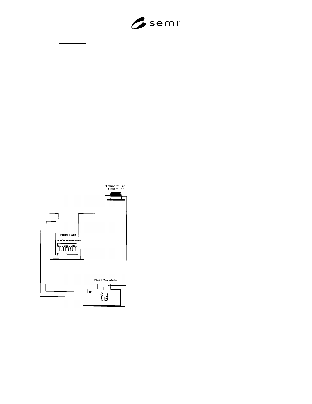
Figure 1
Temperature Controlled Fluid Bath Assembly
NOTICE: These standards do not purport to address
safety issues, if any, associated with their use. It is the
responsibility of the user of these standards to establish
appropriate safety and health practices and determine
the applicability of regulatory limitations prior to use.
SEMI makes no warranties or representations as to the
suitability of the standards set forth herein for any
particular application. The determination of the
suitability of the standard is solely the responsibility of
the user. Users are cautioned to refer to manufacturer’s
instructions, product labels, product data sheets, and
other relevant literature respecting any materials
mentioned herein. These standards are subject to
change without notice.
The user’s attention is called to the possibility that
compliance with this standard may require use of
copyrighted material or of an invention covered by
patent rights. By publication of this standard, SEMI
takes no position respecting the validity of any patent
rights or copyrights asserted in connection with any
item mentioned in this standard. Users of this standard
are expressly advised that determination of any such
patent rights or copyrights, and the risk of infringement
of such rights, are entirely their own responsibility.
Copyright by SEMI® (Semiconductor Equipment and Materials
International), 3081 Zanker Road, San Jose, CA 95134. Reproduction o
f
the contents in whole or in part is forbidden without express written
consent of SEMI.

SEMI G44-94 © SEMI 1986, 19941
SEMI G44-94
SPECIFICATION FOR LEAD FINISHES FOR GLASS TO METAL SEAL
CERAMIC PACKAGES (ACTIVE DEVICES ONLY)
1 Preface
1.1 This specification defines lead finishes for glass to
metal seal ceramic packages assembled with iron-nickel
alloy leadframe construction. It defines composition,
properties, limits, and refers to appropriate tests for
utility.
1.2 Scope — The criteria detailed in this document
applies to glass to metal seal ceramic packages,
assembled with iron-nickel alloy leadframe
construction, which conforms to composition limits
specified in MIL-M-38510 as lead material Type A or
Type B.
1.3 Units — U.S. Customary (inch -pound) or metric
(SI) units may be used at the customer’s discretion.
This specification uses U.S. Customary units as the
prime unit.
2 Applicable Documents
2.1 Order of Precedence — To avoid conflicts, the
order of precedence when ordering packages shall be as
follows:
Purchase Order
Customer Package Drawing
This Specification
Reference Documents
Related Documents
2.1.1 SEMI Specifications
SEMI G2 — Specification; Metallic Leadframes for
Cer-DIP Packages
SEMI G35 — Specification; Test Methods for Lead
Finishes on Semiconductor (Active Devices)
2.1.2 ASTM Specifications
1
B 487 — Measuring Metal and Oxide Coating
Thickness by Microscopical Examination of a Cross
Section
B 545 — Standard Specification for Electro-deposited
Coatings of Tin
B 567 — Measurement of Coating Thickness by the
Beta Backscatter Principle
1 American Society for Testing and Materials, 100 Barr Harbor
Drive, West Conshohoken, PA 19428-2959
B 568 — Measurement for Coating Thickness by X-
Ray Spectrometry
B 571 — Adhesion of Metallic Coatings
E 384 — Standard Test Methods for Micro-hardness of
Materials
2.1.3 Federal Specification
2
QQ-S-571 — Solder, Tin Alloy; Tin-Lead Alloy; and
Lead (Pb) Alloy
2.2 Military Specifications
2
MIL-T-10727 — Tin Plating; Electrodeposits or Hot
Dipped, for Ferrous and Non-Ferrous Metals
MIL-G-45204 — Gold Plating, Electrodeposited
MIL-STD-883 — Test Methods and Procedures for
Microelectronics
MIL-M-38510 — Microcircuits, General Specification
3 Terminology
blister — An enclosed localized separation of the
plating from its base metal or an underplated layer that
does not expose the underlying layer.
pit — A shallow depression or crater. The bottom of the
depression must be visible.
solder — As used in this specification, refers to tin lead
(Pb) as 63/37 or 60/40, unless otherwise specified and
agreed upon between user and supplier and stated on
procurement drawings.
4 Dimensions and Material
Composition limits, mechanical and physical
properties, dimensions and tolerances for Cer-DIP
leadframes are as stated in SEMI G2.
Table 1 lists recommended finishes for devices
employing iron nickel alloy leadframe (MIL-M-38510
Lead Material Type A or Type B).
Gold plate is useable in socketed applications as well as
in soldered applications. Hardness, grain size, and other
properties shall be specified in the procurement
drawing.
2 Military Standards, Naval Publications and Form Center, 5801
Tabor Avenue, Philadelphia, PA 19120